JAJSK31G October 2020 – September 2023 REF70
PRODMIX
- 1
- 1 特長
- 2 アプリケーション
- 3 概要
- 4 Revision History
- 5 Device Comparison Table
- 6 Pin Configuration and Functions
-
7 Specifications
- 7.1 Absolute Maximum Ratings
- 7.2 ESD Ratings
- 7.3 Recommended Operating Conditions
- 7.4 Thermal Information
- 7.5 REF7012 Electrical Characteristics
- 7.6 REF7025 Electrical Characteristics
- 7.7 REF7030 Electrical Characteristics
- 7.8 REF7033 Electrical Characteristics
- 7.9 REF7040 Electrical Characteristics
- 7.10 REF7050 Electrical Characteristics
- 7.11 Typical Characteristics
- 8 Parameter Measurement Information
- 9 Detailed Description
- 10Application and Implementation
- 11Device and Documentation Support
- 12Mechanical, Packaging, and Orderable Information
パッケージ・オプション
メカニカル・データ(パッケージ|ピン)
サーマルパッド・メカニカル・データ
発注情報
10.2.2 Typical Application: DAC Force and Sense Reference Drive Circuit
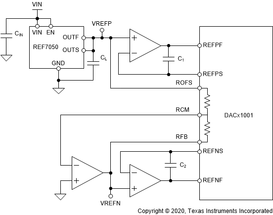
Certain DACs require external voltage references to operate properly. There are DACs that only require a positive voltage for operating in which the basic connection will work. For other DACs there can be a need a positive and negative reference voltage due to their bipolar output.
The circuit shown in Figure 10-3 shows a DAC force and sense reference drive circuit for the DACx1001 using the REF70. This circuit takes advantage of the DACx1001 RCM circuit to remove the need of additional external resistors to make a negative reference due to the integrated precision resistors. This circuit requires additional buffers due to undesired series resistance on the reference input of the DAC.
 Figure 10-3 Basic Force and Sense
Reference Drive Circuit Connections with DACx1001