JAJSK31G October 2020 – September 2023 REF70
PRODMIX
- 1
- 1 特長
- 2 アプリケーション
- 3 概要
- 4 Revision History
- 5 Device Comparison Table
- 6 Pin Configuration and Functions
-
7 Specifications
- 7.1 Absolute Maximum Ratings
- 7.2 ESD Ratings
- 7.3 Recommended Operating Conditions
- 7.4 Thermal Information
- 7.5 REF7012 Electrical Characteristics
- 7.6 REF7025 Electrical Characteristics
- 7.7 REF7030 Electrical Characteristics
- 7.8 REF7033 Electrical Characteristics
- 7.9 REF7040 Electrical Characteristics
- 7.10 REF7050 Electrical Characteristics
- 7.11 Typical Characteristics
- 8 Parameter Measurement Information
- 9 Detailed Description
- 10Application and Implementation
- 11Device and Documentation Support
- 12Mechanical, Packaging, and Orderable Information
パッケージ・オプション
メカニカル・データ(パッケージ|ピン)
サーマルパッド・メカニカル・データ
発注情報
10.3 Power Supply Recommendation
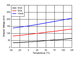
The REF70 family of references features a low-dropout voltage. These references can be operated with a supply of only 50 mV above the output voltage for 0-mA output current conditions. The dropout voltage will vary with the output current so refer to the dropout voltage to see typical dropout voltage requirements. TI recommends a supply bypass capacitor ranging between 0.1 µF to 10 µF.
During start-up the REF70 can experience moments of high input current due to the output capacitors. The input current can momentarily rise to ISC.
 Figure 10-6 Dropout Voltage vs Temperature