JAJSR00F October 1995 – February 2024 SN54AC373 , SN74AC373
PRODUCTION DATA
- 1
- 1 特長
- 2 概要
- 3 Pin Configuration and Functions
-
4 Specifications
- 4.1 Absolute Maximum Ratings
- 4.2 Recommended Operating Conditions
- 4.3 Thermal Information
- 4.4 Electrical Characteristics
- 4.5 Timing Requirements, VCC = 3.3 V ± 0.3 V
- 4.6 Timing Requirements, VCC = 5 V ± 0.5 V
- 4.7 Switching Characteristics, VCC = 3.3 V ± 0.3 V
- 4.8 Switching Characteristics, VCC = 5 V ± 0.5 V
- 4.9 Operating Characteristics
- 5 Parameter Measurement Information
- 6 Detailed Description
- 7 Application and Implementation
- 8 Device and Documentation Support
- 9 Revision History
- 10Mechanical, Packaging, and Orderable Information
パッケージ・オプション
デバイスごとのパッケージ図は、PDF版データシートをご参照ください。
メカニカル・データ(パッケージ|ピン)
- W|20
- J|20
- FK|20
サーマルパッド・メカニカル・データ
発注情報
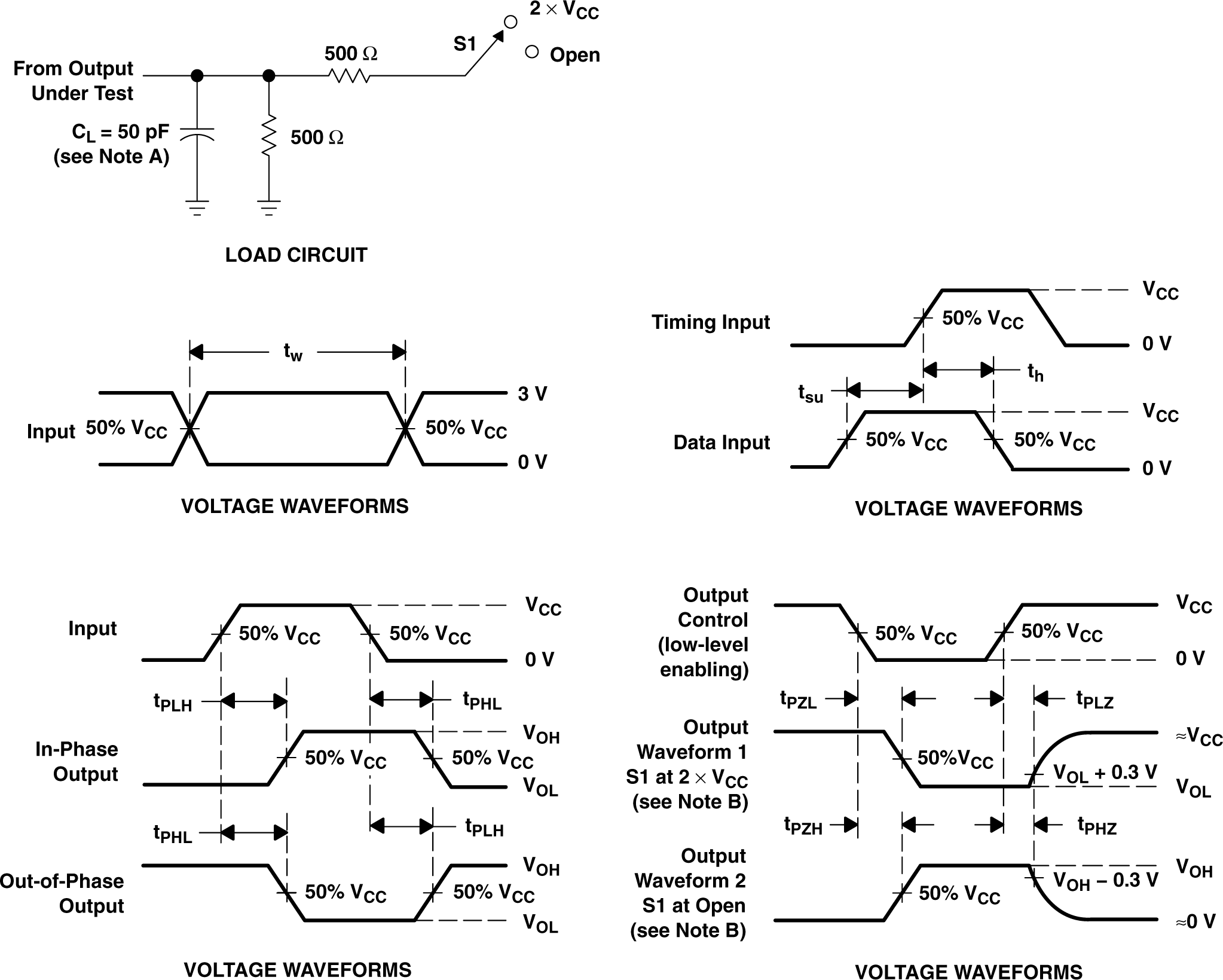
5 Parameter Measurement Information

A. CL includes probe and jig capacitance.
B. Waveform 1 is for an output with internal conditions such that the output is low except when disabled by the output control. Waveform 2 is for an output with internal conditions such that the output is high except when disabled by the output control.
C. All input pulses are supplied by generators having the following characteristics: PRR ≤ 1 MHz, ZO = 50 Ω, tr ≤ 2.5 ns, tf ≤ 2.5 ns.
D. The outputs are measured one at a time with one input transition per measurement.
Figure 5-1 Load Circuit and Voltage Waveforms| TEST | S1 |
|---|---|
| tPLH/tPHL | Open |
| tPLZ/tPZL | 2 × VCC |
| tPHZ/tPZH | Open |