SDLS146B October 1976 – September 2016 SN54LS245 , SN74LS245
- 1 Features
- 2 Applications
- 3 Description
- 4 Revision History
- 5 Device Comparison Table
- 6 Pin Configuration and Functions
- 7 Specifications
- 8 Parameter Measurement Information
- 9 Detailed Description
- 10Application and Implementation
- 11Power Supply Recommendations
- 12Layout
- 13Device and Documentation Support
- 14Mechanical, Packaging, and Orderable Information
パッケージ・オプション
デバイスごとのパッケージ図は、PDF版データシートをご参照ください。
メカニカル・データ(パッケージ|ピン)
- W|20
サーマルパッド・メカニカル・データ
発注情報
9 Detailed Description
9.1 Overview
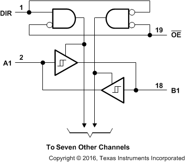
The SNx4LS245 uses Schottky transistor logic to perform the standard '245 transceiver function. This standard logic function has a common pinout, direction select pin, and active-low output enable. When the outputs are disabled, the A and B sides of the device are effectively isolated.
9.2 Functional Block Diagram
 Figure 3. Logic Diagram (Positive Logic)
9.3 Feature Description
9.3.1 3-State outputs
The 3-state outputs can drive bus lines directly. All outputs can be put into high impedance mode through the OE pin.
9.3.2 PNP Inputs
This device has PNP inputs which reduce dc loading on bus lines.
9.3.3 Hysteresis on Bus Inputs
The bus inputs have built-in hysteresis that improves noise margins.
9.4 Device Functional Modes
The SNx4LS245 performs the standard '245 logic function. Data can be transmitted from A to B or from B to A depending on the DIR pin value, or the A and B sides can be isolated from one another by setting the OE pin HIGH.
Table 1. Function Table
| INPUTS | OPERATION | |
|---|---|---|
| OE | DIR | |
| L | L | B data to A bus |
| L | H | A data to B bus |
| H | X | Isolation |
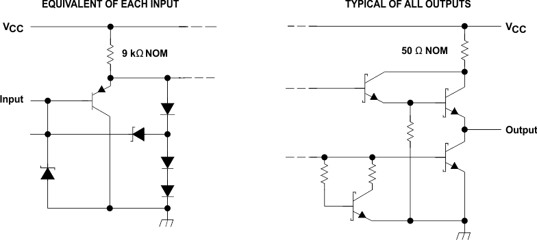
 Figure 4. Schematics of Inputs and Outputs