JAJSUL0P January   1993  – May 2024 SN54LVC257A , SN74LVC257A

PRODUCTION DATA  

  1.   1
  2. 特長
  3. アプリケーション
  4. 概要
  5. Pin Configuration and Functions
  6. Specifications
    1. 5.1 Absolute Maximum Ratings
    2. 5.2 ESD Ratings
    3. 5.3 Recommended Operating Conditions
    4. 5.4 Thermal Information
    5. 5.5 Electrical Characteristics
    6. 5.6 Switching Characteristics, SN54LVC257A
    7. 5.7 Switching Characteristics, SN74LVC257A
    8. 5.8 Operating Characteristics
    9. 5.9 Typical Characteristics
  7. Parameter Measurement Information
  8. Detailed Description
    1. 7.1 Overview
    2. 7.2 Functional Block Diagram
    3. 7.3 Feature Description
    4. 7.4 Device Functional Modes
  9.   Application and Implementation
    1. 8.1 Application Information
    2. 8.2 Typical Application
      1. 8.2.1 Design Requirements
      2. 8.2.2 Detailed Design Procedure
      3. 8.2.3 Application Curves
    3. 8.3 Power Supply Recommendations
    4. 8.4 Layout
      1. 8.4.1 Layout Guidelines
      2. 8.4.2 Layout Example
  10. Device and Documentation Support
    1. 8.1 Documentation Support (Analog)
      1. 8.1.1 Related Documentation
      2. 8.1.2 Related Links
    2. 8.2 Community Resources
    3. 8.3 ドキュメントの更新通知を受け取る方法
    4. 8.4 サポート・リソース
    5. 8.5 Trademarks
    6. 8.6 静電気放電に関する注意事項
    7. 8.7 用語集
  11. Revision History
  12. 10Mechanical, Packaging, and Orderable Information

パッケージ・オプション

メカニカル・データ(パッケージ|ピン)
サーマルパッド・メカニカル・データ
発注情報

Typical Application

The SNx4LVC257A devices use CMOS technology and have balanced output drive. These devices can be used for down level translation and multiplexer function as shown in Figure 8-1.
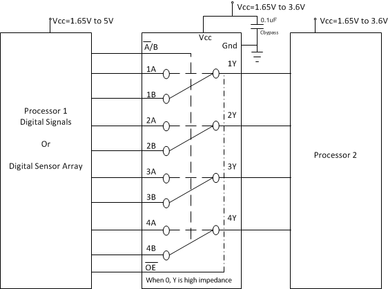
SN54LVC257A SN74LVC257A SNx4LVC257A Used as Level Translation and as a MultiplexerFigure 8-1 SNx4LVC257A Used as Level Translation and as a Multiplexer