JAJSPA1I June 1999 – October 2022 SN65C3243 , SN75C3243
PRODUCTION DATA
- 1 特長
- 2 アプリケーション
- 3 概要
- 4 Revision History
- 5 Pin Configuration and Functions
-
6 Specifications
- 6.1 Absolute Maximum Ratings
- 6.2 ESD Ratings
- 6.3 Recommended Operating Conditions
- 6.4 Thermal Information
- 6.5 Electrical Characteristics
- 6.6 Electrical Characteristics, Driver Section
- 6.7 Electrical Characteristics, Receiver Section
- 6.8 Electrical Characteristics, Auto-Powerdown Section
- 6.9 Switching Characteristics: Driver
- 6.10 Switching Characteristics: Receiver
- 6.11 Switching Characteristics: Auto-Powerdown
- 7 Parameter Measurement Information
- 8 Detailed Description
- 9 Device and Documentation Support
- 10Mechanical, Packaging, and Orderable Information
パッケージ・オプション
メカニカル・データ(パッケージ|ピン)
サーマルパッド・メカニカル・データ
- DW|28
発注情報
7 Parameter Measurement Information

A. CL includes probe
and jig capacitance.
B. The pulse generator has the
following characteristics: PRR = 1 Mbits, ZO = 50 Ω , 50% duty
cycle, tr ≤ 10 ns, tf ≤ 10 ns.
Figure 7-1 Driver Slew Rate
A. CL includes probe
and jig capacitance.
B. The pulse generator has the
following characteristics: PRR = 1 Mbits, ZO = 50 Ω , 50% duty
cycle, tr ≤ 10 ns, tf ≤ 10 ns.
Figure 7-2 Driver Pulse Skew
A. CL includes probe
and jig capacitance.
B. The pulse generator has the
following characteristics: ZO = 50 Ω , 50% duty cycle,
tr ≤ 10 ns, tf ≤ 10 ns.
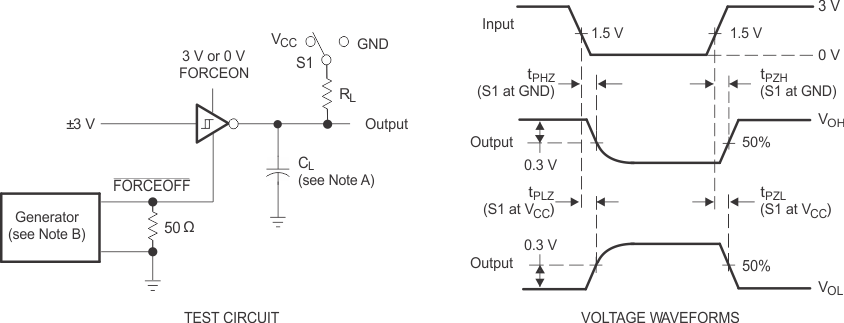
Figure 7-3 Receiver Propagation Delay Times
A. CL includes probe
and jig capacitance.
B. The pulse generator has the
following characteristics: ZO = 50 Ω , 50% duty cycle,
tr ≤ 10 ns, tf ≤ 10 ns.
C. tPLZ and
tPHZ are the same as tdis.
D. tPZL and
tPZH are the same as ten.
Figure 7-4 Receiver Enable and Disable Times
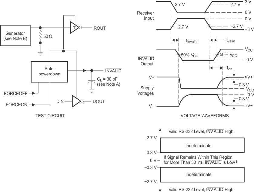
A. CL includes probe
and jig capacitance.
B. The pulse generator has the
following characteristics: PRR = 5 Mbits, ZO = 50 Ω , 50% duty
cycle, tr ≤ 10 ns, tf ≤ 10 ns.
Figure 7-5 INVALID Propagation Delay Times and Supply
Enabling Time
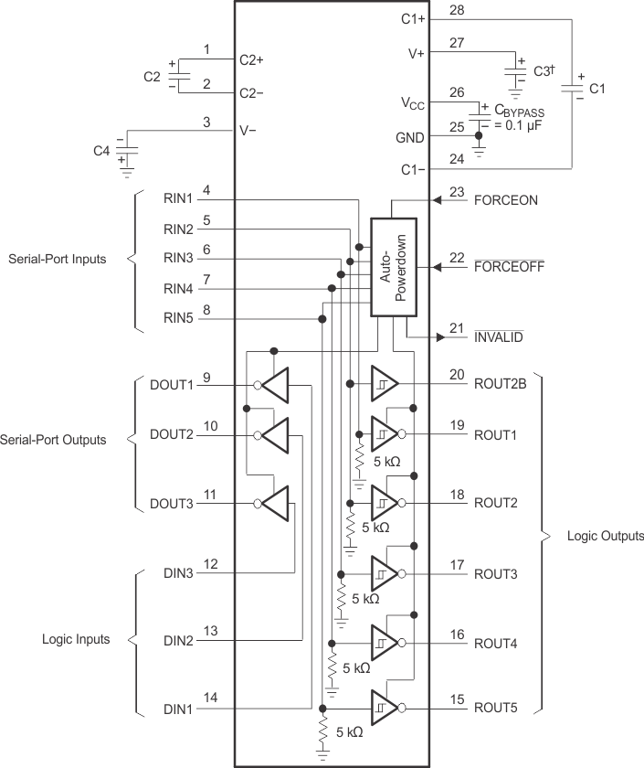
† C3 can be
connected to VCC or GND.
A. Resistor values shown are
nominal.
Figure 7-6 Typical Operating Circuit and Capacitor ValuesTable 7-1 VCC vs
Capacitor Values
| VCC | C1 | C2, C3, and C4 |
|---|---|---|
| 3.3 V ± 0.3 V | 0.1 µF | 0.1 µF |
| 5 V ± 0.5 V | 0.047 µF | 0.33 µF |
| 3 V to 5.5 V | 0.1 µF | 0.47 µF |