JAJSFO2I
september 2012 – october 2020
SN65DSI83
PRODUCTION DATA
1
1
特長
2
アプリケーション
3
概要
4
Revision History
5
Pin Configuration and Functions
6
Specifications
6.1
Absolute Maximum Ratings #GUID-BDB96F65-5C5F-4805-AA4B-B71B15ADA38F/SLLSEB91839
6.2
ESD Ratings
6.3
Recommended Operating Conditions
6.4
Thermal Information
6.5
Electrical Characteristics
6.6
Timing Requirements
6.7
Switching Characteristics
7
Detailed Description
7.1
Overview
7.2
Functional Block Diagram
7.3
Feature Description
7.3.1
Clock Configurations and Multipliers
7.3.2
ULPS
7.3.3
LVDS Pattern Generation
7.4
Device Functional Modes
7.4.1
Reset Implementation
7.4.2
Initialization Sequence
7.4.3
LVDS Output Formats
7.4.4
DSI Lane Merging
7.4.5
DSI Pixel Stream Packets
7.4.6
DSI Video Transmission Specifications
7.5
Programming
7.5.1
Local I2C Interface Overview
7.6
Register Maps
7.6.1
Control and Status Registers Overview
8
Application and Implementation
8.1
Application Information
8.1.1
Video STOP and Restart Sequence
8.1.2
Reverse LVDS Pin Order Option
8.1.3
IRQ Usage
8.2
Typical Application
8.2.1
Design Requirements
8.2.2
Detailed Design Procedure
8.2.2.1
Example Script
8.2.3
Application Curve
9
Power Supply Recommendations
9.1
VCC Power Supply
9.2
VCORE Power Supply
10
Layout
10.1
Layout Guidelines
10.1.1
Package Specific
10.1.2
Differential Pairs
10.1.3
Ground
10.2
Layout Example
11
Device and Documentation Support
11.1
Receiving Notification of Documentation Updates
11.2
Community Resources
11.3
Trademarks
Mechanical, Packaging, and Orderable Information
パッケージ・オプション
メカニカル・データ(パッケージ|ピン)
ZXH|64
MPBGAK9A
サーマルパッド・メカニカル・データ
発注情報
jajsfo2i_oa
jajsfo2i_pm
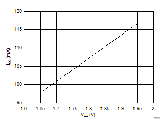
8.2.3
Application Curve
A.
All typical values are at T
A
= 25°C.
B.
SN65DSI83: SINGLE Channel DSI to SINGLE Channel DSI, 1280 × 800
number of LVDS lanes = 3 data lanes + 1 CLK lane
number of DSI lanes = 4 data lanes + 1 CLK lane
LVDS CLK OUT = 83 M
DSI CLK = 500 M
RGB666, LVDS 18 bpp
Figure 8-2
Power Consumption