JAJSPZ7E november   2002  – march 2023 SN65HVD08 , SN75HVD08

PRODUCTION DATA  

  1. 特長
  2. アプリケーション
  3. 説明
  4. Revision History
  5. Pin Configuration and Functions
  6. Specifications
    1. 6.1 Absolute Maximum Ratings
    2. 6.2 ESD Ratings
    3. 6.3 Recommended Operating Conditions
    4. 6.4 Thermal Information
    5. 6.5 Electrical Characteristics
    6. 6.6 Driver Switching Characteristics
    7. 6.7 Receiver Switching Characteristics
    8. 6.8 Typical Characteristics
  7. Parameter Measurement Information
  8. Detailed Description
    1. 8.1 Overview
    2. 8.2 Functional Block Diagram
    3. 8.3 Feature Description
    4. 8.4 Device Functional Modes
  9. Application and Implementation
    1. 9.1 Application Information
      1. 9.1.1 Supply Source Impedance
      2. 9.1.2 Opto-Isolated Data Buses
      3. 9.1.3 Opto Alternative
    2. 9.2 Typical Application
      1. 9.2.1 Design Requirements
        1. 9.2.1.1 Data Rate and Bus Length
        2. 9.2.1.2 Stub Length
          1.        30
          2.        31
        3. 9.2.1.3 Bus Loading
        4. 9.2.1.4 Receiver Failsafe
      2. 9.2.2 Detailed Design Procedure
      3. 9.2.3 Application Curve
    3. 9.3 Power Supply Recommendations
    4. 9.4 Layout
      1. 9.4.1 Layout Guidelines
      2. 9.4.2 Layout Example
  10. 10Device and Documentation Support
    1. 10.1 Device Support
      1. 10.1.1 サード・パーティ製品に関する免責事項
    2. 10.2 サポート・リソース
    3. 10.3 Trademarks
    4. 10.4 静電気放電に関する注意事項
    5. 10.5 用語集
  11. 11Mechanical, Packaging, and Orderable Information

パッケージ・オプション

メカニカル・データ(パッケージ|ピン)
サーマルパッド・メカニカル・データ
発注情報

Typical Characteristics

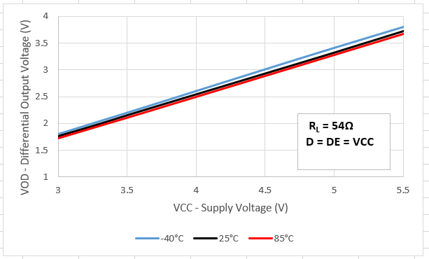
GUID-20230303-SS0I-LSK1-33D3-WHRSWGJSWQ1X-low.pngFigure 6-2 Differential Output Voltage vs Supply Voltage
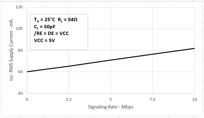
GUID-20230303-SS0I-HNNM-RWQ9-7P10FZDPTJ3Q-low.pngFigure 6-4 RMS Supply Current vs Signaling Rate
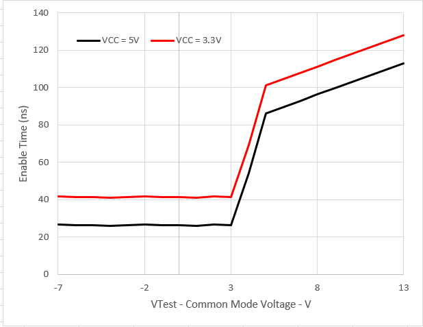
GUID-20230303-SS0I-N4GV-0MQG-SLSCZDMD4RND-low.pngFigure 6-6 Enable Time vs Common-Mode Voltage (See Figure 6-1)
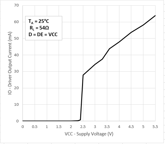
GUID-20230303-SS0I-WVNV-4KHB-VX82B6LH73V4-low.pngFigure 6-3 Driver Output Current vs Supply Voltage
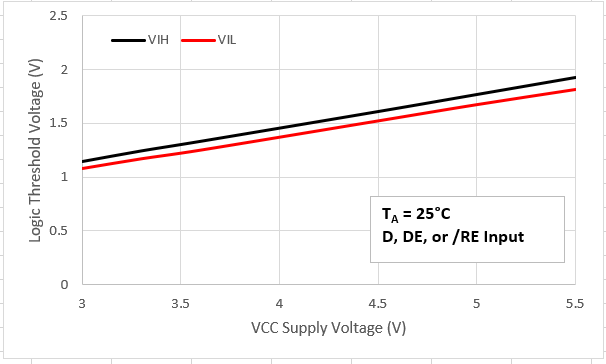
GUID-20230303-SS0I-7GDG-HDWM-6B9GG8SRQ4LF-low.pngFigure 6-5 Logic Input Threshold Voltage vs Supply Voltage