-
SN65HVD10x IO-Link PHY for Device Nodes SLLSE84D May 2011 – May 2017 SN65HVD101 , SN65HVD102
PRODUCTION DATA.
-
SN65HVD10x IO-Link PHY for Device Nodes
- 1 Features
- 2 Applications
- 3 Description
- 4 Revision History
- 5 Device Comparison Table
- 6 Pin Configuration and Functions
- 7 Specifications
- 8 Parameter Measurement
-
9 Detailed Description
- 9.1 Overview
- 9.2 Functional Block Diagram
- 9.3
Feature Description
- 9.3.1 Wake-up Detection
- 9.3.2 Current Limit Indication - Short Circuit Current Detection
- 9.3.3 Active Current Limit Condition: VTHL > VCQ ≥ VTHH
- 9.3.4 Inactive Current Limit Condition: VTHL < VCQ < VTHH
- 9.3.5 Over-temperature Detection
- 9.3.6 CQ Current-limit Adjustment
- 9.3.7 Transceiver Function Tables
- 9.3.8 Voltage Regulator (Not Available in SN65HVD102)
- 9.4 Device Functional Modes
- 10Application and Implementation
- 11Power Supply Recommendations
- 12Layout
- 13Device and Documentation Support
- 14Mechanical, Packaging, and Orderable Information
- IMPORTANT NOTICE
パッケージ・オプション
メカニカル・データ(パッケージ|ピン)
- RGB|20
サーマルパッド・メカニカル・データ
- RGB|20
発注情報
SN65HVD10x IO-Link PHY for Device Nodes
1 Features
- Configurable CQ Output: Push-Pull, High-Side, or Low-Side for SIO Mode
- Remote Wake-Up Indicator
- Current Limit Indicator
- Power-Good Indicator
- Overtemperature Protection
- Reverse Polarity Protection
- Configurable Current Limits
- 9-V to 36-V Supply Range
- Tolerant to 50-V Peak Line Voltage
- 3.3-V/5-V Configurable Integrated LDO (SN65HVD101 ONLY)
- 20-pin QFN Package, 4 mm × 3.5 mm
2 Applications
- Suitable for IO-Link Device Nodes
3 Description
The SN65HVD101 and ‘HVD102 IO-Link PHYs implement the IO-Link interface for industrial point-to-point communication. When the device is connected to an IO-Link master through a 3-wire interface, the master can initiate communication and exchange data with the remote node while the SN65HVD10X acts as a complete physical layer for the communication.
The IO-Link driver output (CQ) can be used in push-pull, high-side, or low-side configurations using the EN and TX input pins. The PHY receiver converts the 24-V IO-Link signal on the CQ pin to standard logic levels on the RX pin. A simple parallel interface is used to receive and transmit data and status information between the PHY and the local controller.
The SN65HVD101 and 'HVD102 implement protection features for overcurrent, overvoltage and overtemperature conditions. The IO-Link driver current limit can be set using an external resistor. If a short-circuit current fault occurs, the driver outputs are internally limited, and the PHY generates an error signal (SC). These devices also implement an overtemperature shutdown feature that protects the device from high-temperature faults.
The SN65HVD102 operates from a single external 3.3-V or 5-V local supply. The SN65HVD101 integrates a linear regulator that generates either 3.3 V or 5 V from the IO-Link L+ voltage for supplying power to the PHY as well as a local controller and additional circuits.
The SN65HVD101 and 'HVD102 are available in the 20-pin RGB package (4 mm × 3,5 mm QFN) for space-constrained applications.
Device Information(1)
| PART NUMBER | PACKAGE | BODY SIZE (NOM) |
|---|---|---|
| SN65HVD101 | QFN (20) | 4.00 mm × 3.50 mm |
| SN65HVD102 |
- For all available packages, see the orderable addendum at the end of the data sheet.
4 Revision History
Changes from C Revision (February 2017) to D Revision
- Changed From: 950 mW To: 950 W, and From: 475 mW To: 475 W in the TVS Evaluation section Go
Changes from B Revision (April 2015) to C Revision
- Changed pin 1 of the SN65HVD102 From: nc To: Vcc SET Go
Changes from A Revision (March 2013) to B Revision
- Added Device Information and ESD Rating tables, Feature Description section, Device Functional Modes, Application and Implementation section, Power Supply Recommendations section, Layout section, Device and Documentation Support section, and Mechanical, Packaging, and Orderable Information section. Go
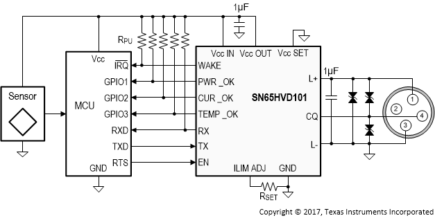
- Changed front-page Simplified Schematic image. Go
- Changed Pin Functions table format Go
- Re-write detailed description section. Go
- Re-write application information section. Go
Changes from * Revision (May 2011) to A Revision
- Changed the devices From: Product Preview To: ProductionGo
5 Device Comparison Table
| DEVICE | VOLTAGE REGULATOR |
|---|---|
| SN65HVD101 | Yes |
| SN65HVD102 | No |
6 Pin Configuration and Functions

Pin Functions
| PIN | DESCRIPTION | ||
|---|---|---|---|
| NAME | NUMBER | TYPE(1) | |
| IO-Link Interface | |||
| L+ | 10 | P | IO-Link supply voltage (24V nominal) |
| CQ | 12 | I/O | IO-Link data signal (bi-directional) |
| L– | 14 | P | IO-Link ground (connect to board ground) |
| Local Controller Interface | |||
| CUR_OK | 15 | OD | High-CQ-current fault indicator output signal from PHY to the microcontroller. Connect this pin via pull-up resistor to Vcc OUT. A LOW level indicates over-current condition. |
| WAKE | 16 | OD | Wake up indicator from the PHY to the local controller Connect this pin via pull-up resistor to Vcc OUT. |
| RX | 17 | O | PHY receive data output to the local controller |
| TX | 18 | I | PHY transmit data input from the local controller |
| EN | 20 | I | Driver enable input signal from the local controller |
| Power Supply Pins | |||
| VCC IN | 7 | A | Voltage supply input for SN65HVD102 Voltage sense feedback input for the voltage regulator of the SN65HVD101. Connect this pin to pin 8 either directly or through a current boost transistor. |
| VCC OUT | 8 | P | Not connected in SN65HVD102 Linear regulator output of SN65HVD101. Connect this pin to pin 7 either directly or through a current boost transistor. |
| GND | 3, 6, 13 | P | Logic ground potential |
| Special Connect Pins | |||
| VCC SET | 1 | I | Connect this pin to ground to make Vcc OUT = 3.3V. Leave this pin floating to make Vcc OUT = 5V. |
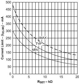
| ILIMADJ | 4 | A | Input for current limit adjustment. Connect resistor RSET between this pin and ground. For RSET values see Figure 2. |
| PWR_OK | 5 | OD | Power-Good indicator. Connect this pin via pull-up resistor to Vcc OUT. A HIGH at this pin indicates that L+ and Vcc OUT are at correct levels. |
| Temp_OK | 19 | OD | Temperature-Good indicator. Connect this pin via pull-up resistor to Vcc OUT. High-impedance at this pin indicates that the internal temperature is at a safe level. A low at this pin indicates the device is approaching thermal shutdown. |
| NC | 2, 9, 11 | – | No Connection. Leave these pins floating (open) |
7 Specifications
7.1 Absolute Maximum Ratings
over operating free-air temperature range (unless otherwise noted) (1)| MIN | MAX | UNIT | |||
|---|---|---|---|---|---|
| Line voltage | L+, CQ | Steady state | –40 | 40(2) (3) | V |
| Transient pulse width <100 µs | –50 | 50 | V | ||
| Voltage difference | |VL+ – VCQ| | 40 | |||
| Supply voltage | VCC | –0.3 | 6 | V | |
| Input voltage | TX, EN, VCC_SET, ILIMADJ, | –0.3 | 6 | V | |
| Output voltage | RX, CUR_OK, WAKE, PWR_OK | –0.3 | 6 | V | |
| Output current | RX, CUR_OK, WAKE, PWR_OK | –5 | 5 | mA | |
| Storage temperature, Tstg | –65 | 150 | °C | ||
| Junction temperature, TJ | 180 | °C | |||
7.2 ESD Ratings
| VALUE | UNIT | |||
|---|---|---|---|---|
| V(ESD) | Electrostatic discharge | Human-body model (HBM, all pins), per ANSI/ESDA/JEDEC JS-001(1) | ±2000 | V |
7.3 Recommended Operating Conditions
| MIN | NOM | MAX | UNIT | |||
|---|---|---|---|---|---|---|
| VL+ | Line voltage(1) | 9 | 24 | 30 | V | |
| VCC | Logic supply voltage (3.3V nominal) | 3 | 3.3 | 3.6 | V | |
| VCC | Logic supply voltage (5V nominal) | 4.5 | 5 | 5.5 | V | |
| VIL | Logic low input voltage | 0.8 | V | |||
| VIH | Logic high input voltage | 2 | V | |||
| IO | Logic output current | –4 | 4 | mA | ||
| ICC(OUT) | Logic supply current (HVD101) | 20 | mA | |||
| IO(LIM) | CQ driver output current limit | 100 | 450 | mA | ||
| RSET | External resistor for CQ current limit | 0 | 20 | kΩ | ||
| CCOMP | Compensation capacitor for voltage regulator (HVD101) | 3.3 | µF | |||
| 1/tBIT | Signaling rate | IO-Link mode | 250 | kbps | ||
| SIO mode | 10 | |||||
| TA | Ambient temperature | –40 | 105 | °C | ||
| TJ | Junction temperature | –40 | 150 | °C | ||
7.4 Thermal Information
| THERMAL METRIC(1) | SN65HVD10x | UNITS | |
|---|---|---|---|
| RGB 20 PINS | |||
| RθJA | Junction-to-ambient thermal resistance | 33.8 | °C/W |
| RθJC(top) | Junction-to-case (top) thermal resistance | 36.6 | |
| RθJB | Junction-to-board thermal resistance | 10.3 | |
| ψJT | Junction-to-top characterization parameter | 0.4 | |
| ψJB | Junction-to-board characterization parameter | 10.3 | |
| RθJC(bot) | Junction-to-case (bottom) thermal resistance | 2.3 | |
7.5 Electrical Characteristics
over all operating conditions (unless otherwise noted)| PARAMETER | TEST CONDITIONS | MIN | TYP | MAX | UNIT | ||||
|---|---|---|---|---|---|---|---|---|---|
| Driver | |||||||||
| IIN | Input current (TX, EN) | VIN = 0V to VCC | –100 | 100 | µA | ||||
| VRQH | Residual voltage across the driver high side switch | ICQ = –250 mA | 18 < VL+ | 1.5 | 3 | V | |||
| VL+ < 18 | 3.5 | V | |||||||
| ICQ = –200 mA | 18 < VL+ | 2 | V | ||||||
| VL+ < 18 | 2.5 | V | |||||||
| VRQL | Residual voltage across the driver low side switch | ICQ = 250 mA | 18 < VL+ | 1.5 | 3 | V | |||
| VL+ < 18 | 3.5 | V | |||||||
| ICQ = 200 mA | 18 < VL+ | 2 | V | ||||||
| VL+ < 18 | 2.5 | V | |||||||
| |IO(LIM)| | Driver output current limit | RSET = 20 kΩ | 60 | 95 | 130 | mA | |||
| RSET = 0 kΩ | 300 | 400 | 480 | mA | |||||
| I(OZ) | CQ leakage current with EN = L | VCQ = 8 V | –2 | 2 | µA | ||||
| Receiver | |||||||||
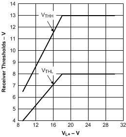
| VTHH | Input threshold “H” | 18 V < VL+ < 30 V | 10.5 | 13 | V | ||||
| VTHL | Input threshold “L” | 8 | 11.5 | V | |||||
| VHYS | Receiver Hysteresis (VTHH – VTHL) | 0.5 | 1 | V | |||||
| VTHH | Input threshold “H” | 9 V < VL+ < 18 V | Note (1) | Note(2) | V | ||||
| VTHL | Input threshold “L” | Note (3) | Note(4) | V | |||||
| VHYS | Receiver Hysteresis (VTHH–VTHL) | 0.25 | V | ||||||
| VOL | Output low voltage | RX | IOL = 4 mA | 0.4 | V | ||||
| OD outputs | IOL = 1 mA | 0.4 | |||||||
| VOH | Output high voltage | RX | IOH = –4 mA | VCC–0.5 | V | ||||
| IOZ | Output leakage current | OD outputs | Output in Z state, VO = VCC | 0.03 | 1 | µA | |||
| Protection Thresholds | |||||||||
| VPG1 | VL+ threshold for PWR_OK | 8 | 10 | V | |||||
| VPG2 | VCC threshold for PWR_OK | VCC Set = GND | 2.45 | 2.75 | 3 | V | |||
| VCC Set = OPEN | 3.9 | 4.25 | 4.6 | ||||||
| VPOR1 | Power-on Reset for VL+ | 6 | V | ||||||
| VPOR2 | Power-on Reset for VCC | 2.5 | V | ||||||
| Voltage Regulator (HVD101) | |||||||||
| VCC_OUT | Voltage regulator output | 9 V < VL+ < 30 V | VCC SET = OPEN | 4.5 | 5 | 5.5 | V | ||
| VCC SET = GND | 3 | 3.3 | 3.6 | ||||||
| VDROP | Voltage regulator drop-out voltage (VL+ – VCC_OUT ) | ICC = 20 mA load current | 3.2 | 3.9 | V | ||||
| Line regulation (dVCC_OUT /dL+) | 9 V < VL+ < 30 V, IVCC = 1 mA | 4 | mV/V | ||||||
| Load regulation (dVCC_OUT /VCC_OUT) | VL+ = 24 V, IVCC = 100 µA to 20 mA |
1.3% | 5% | ||||||
| PSRR | Power Supply Rejection Ratio | 100 kHz, IVCC = 20 mA | 30 | 40 | dB | ||||
| Supply Current | |||||||||
| IL+ | Quiescent supply current | Driver disabled, No Load | HVD102 | 1 | 2 | mA | |||
| HVD101 | 1.3 | 3 | |||||||
| Dynamic supply current | HVD102 | 2 | |||||||
| HVD101 | 1.5 | ||||||||
7.6 Switching Characteristics
over operating free-air temperature range (unless otherwise noted)| PARAMETER | TEST CONDITIONS | MIN | TYP | MAX | UNIT | ||
|---|---|---|---|---|---|---|---|
| Driver | |||||||
| tPLH, tPHL | Driver propagation delay | TX to CQ | Figure 1, Figure 2, Figure 3, RL= 2kΩ CL = 5 nF RSET = 0 Ω |
1 | 2 | µs | |
| tP(skew) | Driver propagation delay skew | 0.2 | µs | ||||
| tPZH, tPZL | Driver enable delay (EN to CQ) | 18 V < VL+ < 30 V | 5 | µs | |||
| 9 V < VL+ < 18 V | 8 | ||||||
| tPHZ, tPLZ | Driver disable delay | 18 V < VL+ < 30 V | 5 | µs | |||
| VL+ < 18 V | 8 | ||||||
| tr, tf | Driver output rise, tall time | 18 V < VL+ | 869 | ns | |||
| |tr – tf| | Difference in rise and fall time | 300 | |||||
| Receiver | |||||||
| tWU1 | Wake-up recognition begin | Figure 6 | 45 | 60 | 75 | µs | |
| tWU2 | Wake-up recognition end | 85 | 100 | 135 | |||
| tpWAKE | Wake-up output delay | 155 | |||||
| tND | Noise suppression time(1) | 250 | ns | ||||
| tPR | Receiver propagation delay | Figure 4 | 18 V < VL+ | 300 | 600 | ns | |
| VL+ < 18 V | 800 | ||||||
| Protection Thresholds | |||||||
| TSD | Shutdown temperature | Die temperature | 160 | 175 | 190 | °C | |
| TRE | Re-enable temperature(2) | 110 | 125 | 140 | |||
| Thermal warning temperature (TEMP_OK) | 120 | 135 | 150 | ||||
| tpSC | Current limit indicator delay | 85 | 175 | µs | |||
7.7 Typical Characteristics


