SLLSE84D May 2011 – May 2017 SN65HVD101 , SN65HVD102
PRODUCTION DATA.
- 1 Features
- 2 Applications
- 3 Description
- 4 Revision History
- 5 Device Comparison Table
- 6 Pin Configuration and Functions
- 7 Specifications
- 8 Parameter Measurement
-
9 Detailed Description
- 9.1 Overview
- 9.2 Functional Block Diagram
- 9.3
Feature Description
- 9.3.1 Wake-up Detection
- 9.3.2 Current Limit Indication - Short Circuit Current Detection
- 9.3.3 Active Current Limit Condition: VTHL > VCQ ≥ VTHH
- 9.3.4 Inactive Current Limit Condition: VTHL < VCQ < VTHH
- 9.3.5 Over-temperature Detection
- 9.3.6 CQ Current-limit Adjustment
- 9.3.7 Transceiver Function Tables
- 9.3.8 Voltage Regulator (Not Available in SN65HVD102)
- 9.4 Device Functional Modes
- 10Application and Implementation
- 11Power Supply Recommendations
- 12Layout
- 13Device and Documentation Support
- 14Mechanical, Packaging, and Orderable Information
パッケージ・オプション
メカニカル・データ(パッケージ|ピン)
- RGB|20
サーマルパッド・メカニカル・データ
- RGB|20
発注情報
7 Specifications
7.1 Absolute Maximum Ratings
over operating free-air temperature range (unless otherwise noted) (1)| MIN | MAX | UNIT | |||
|---|---|---|---|---|---|
| Line voltage | L+, CQ | Steady state | –40 | 40(2) (3) | V |
| Transient pulse width <100 µs | –50 | 50 | V | ||
| Voltage difference | |VL+ – VCQ| | 40 | |||
| Supply voltage | VCC | –0.3 | 6 | V | |
| Input voltage | TX, EN, VCC_SET, ILIMADJ, | –0.3 | 6 | V | |
| Output voltage | RX, CUR_OK, WAKE, PWR_OK | –0.3 | 6 | V | |
| Output current | RX, CUR_OK, WAKE, PWR_OK | –5 | 5 | mA | |
| Storage temperature, Tstg | –65 | 150 | °C | ||
| Junction temperature, TJ | 180 | °C | |||
(1) Stresses beyond those listed under Absolute Maximum Ratings may cause permanent damage to the device. These are stress ratings only, which do not imply functional operation of the device at these or any other conditions beyond those indicated under Recommended Operating Conditions. Exposure to absolute-maximum-rated conditions for extended periods may affect device reliability.
(2) All voltages are with reference to the GND pin, unless otherwise specified.
(3) GND pin and L– line should be at the same DC potential
7.2 ESD Ratings
| VALUE | UNIT | |||
|---|---|---|---|---|
| V(ESD) | Electrostatic discharge | Human-body model (HBM, all pins), per ANSI/ESDA/JEDEC JS-001(1) | ±2000 | V |
(1) JEDEC document JEP155 states that 500-V HBM allows safe manufacturing with a standard ESD control process.
7.3 Recommended Operating Conditions
| MIN | NOM | MAX | UNIT | |||
|---|---|---|---|---|---|---|
| VL+ | Line voltage(1) | 9 | 24 | 30 | V | |
| VCC | Logic supply voltage (3.3V nominal) | 3 | 3.3 | 3.6 | V | |
| VCC | Logic supply voltage (5V nominal) | 4.5 | 5 | 5.5 | V | |
| VIL | Logic low input voltage | 0.8 | V | |||
| VIH | Logic high input voltage | 2 | V | |||
| IO | Logic output current | –4 | 4 | mA | ||
| ICC(OUT) | Logic supply current (HVD101) | 20 | mA | |||
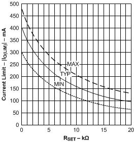
| IO(LIM) | CQ driver output current limit | 100 | 450 | mA | ||
| RSET | External resistor for CQ current limit | 0 | 20 | kΩ | ||
| CCOMP | Compensation capacitor for voltage regulator (HVD101) | 3.3 | µF | |||
| 1/tBIT | Signaling rate | IO-Link mode | 250 | kbps | ||
| SIO mode | 10 | |||||
| TA | Ambient temperature | –40 | 105 | °C | ||
| TJ | Junction temperature | –40 | 150 | °C | ||
(1) These devices will operate with line voltage as low as 9V and as high as 36V, however, the parametric performance is optimized for the IO-Link specified supply voltage range of 18V to 30V.
7.4 Thermal Information
| THERMAL METRIC(1) | SN65HVD10x | UNITS | |
|---|---|---|---|
| RGB 20 PINS | |||
| RθJA | Junction-to-ambient thermal resistance | 33.8 | °C/W |
| RθJC(top) | Junction-to-case (top) thermal resistance | 36.6 | |
| RθJB | Junction-to-board thermal resistance | 10.3 | |
| ψJT | Junction-to-top characterization parameter | 0.4 | |
| ψJB | Junction-to-board characterization parameter | 10.3 | |
| RθJC(bot) | Junction-to-case (bottom) thermal resistance | 2.3 | |
(1) For more information about traditional and new thermal metrics, see the Semiconductor and IC Package Thermal Metrics application report.
7.5 Electrical Characteristics
over all operating conditions (unless otherwise noted)| PARAMETER | TEST CONDITIONS | MIN | TYP | MAX | UNIT | ||||
|---|---|---|---|---|---|---|---|---|---|
| Driver | |||||||||
| IIN | Input current (TX, EN) | VIN = 0V to VCC | –100 | 100 | µA | ||||
| VRQH | Residual voltage across the driver high side switch | ICQ = –250 mA | 18 < VL+ | 1.5 | 3 | V | |||
| VL+ < 18 | 3.5 | V | |||||||
| ICQ = –200 mA | 18 < VL+ | 2 | V | ||||||
| VL+ < 18 | 2.5 | V | |||||||
| VRQL | Residual voltage across the driver low side switch | ICQ = 250 mA | 18 < VL+ | 1.5 | 3 | V | |||
| VL+ < 18 | 3.5 | V | |||||||
| ICQ = 200 mA | 18 < VL+ | 2 | V | ||||||
| VL+ < 18 | 2.5 | V | |||||||
| |IO(LIM)| | Driver output current limit | RSET = 20 kΩ | 60 | 95 | 130 | mA | |||
| RSET = 0 kΩ | 300 | 400 | 480 | mA | |||||
| I(OZ) | CQ leakage current with EN = L | VCQ = 8 V | –2 | 2 | µA | ||||
| Receiver | |||||||||
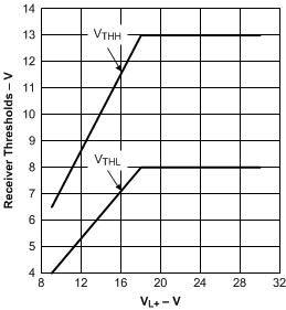
| VTHH | Input threshold “H” | 18 V < VL+ < 30 V | 10.5 | 13 | V | ||||
| VTHL | Input threshold “L” | 8 | 11.5 | V | |||||
| VHYS | Receiver Hysteresis (VTHH – VTHL) | 0.5 | 1 | V | |||||
| VTHH | Input threshold “H” | 9 V < VL+ < 18 V | Note (1) | Note(2) | V | ||||
| VTHL | Input threshold “L” | Note (3) | Note(4) | V | |||||
| VHYS | Receiver Hysteresis (VTHH–VTHL) | 0.25 | V | ||||||
| VOL | Output low voltage | RX | IOL = 4 mA | 0.4 | V | ||||
| OD outputs | IOL = 1 mA | 0.4 | |||||||
| VOH | Output high voltage | RX | IOH = –4 mA | VCC–0.5 | V | ||||
| IOZ | Output leakage current | OD outputs | Output in Z state, VO = VCC | 0.03 | 1 | µA | |||
| Protection Thresholds | |||||||||
| VPG1 | VL+ threshold for PWR_OK | 8 | 10 | V | |||||
| VPG2 | VCC threshold for PWR_OK | VCC Set = GND | 2.45 | 2.75 | 3 | V | |||
| VCC Set = OPEN | 3.9 | 4.25 | 4.6 | ||||||
| VPOR1 | Power-on Reset for VL+ | 6 | V | ||||||
| VPOR2 | Power-on Reset for VCC | 2.5 | V | ||||||
| Voltage Regulator (HVD101) | |||||||||
| VCC_OUT | Voltage regulator output | 9 V < VL+ < 30 V | VCC SET = OPEN | 4.5 | 5 | 5.5 | V | ||
| VCC SET = GND | 3 | 3.3 | 3.6 | ||||||
| VDROP | Voltage regulator drop-out voltage (VL+ – VCC_OUT ) | ICC = 20 mA load current | 3.2 | 3.9 | V | ||||
| Line regulation (dVCC_OUT /dL+) | 9 V < VL+ < 30 V, IVCC = 1 mA | 4 | mV/V | ||||||
| Load regulation (dVCC_OUT /VCC_OUT) | VL+ = 24 V, IVCC = 100 µA to 20 mA |
1.3% | 5% | ||||||
| PSRR | Power Supply Rejection Ratio | 100 kHz, IVCC = 20 mA | 30 | 40 | dB | ||||
| Supply Current | |||||||||
| IL+ | Quiescent supply current | Driver disabled, No Load | HVD102 | 1 | 2 | mA | |||
| HVD101 | 1.3 | 3 | |||||||
| Dynamic supply current | HVD102 | 2 | |||||||
| HVD101 | 1.5 | ||||||||
(1) VTHH(min) = 5V + (11/18)[VL+ - 9V]
(2) VTHH(max) = 6.5V + (13/18)[VL+ - 9V]
(3) VTHL(min) = 4V + (8/18)[VL+ -9V]
(4) VTHL(max) = 6V + (11/18)[VL+ -9V]
7.6 Switching Characteristics
over operating free-air temperature range (unless otherwise noted)| PARAMETER | TEST CONDITIONS | MIN | TYP | MAX | UNIT | ||
|---|---|---|---|---|---|---|---|
| Driver | |||||||
| tPLH, tPHL | Driver propagation delay | TX to CQ | Figure 1, Figure 2, Figure 3, RL= 2kΩ CL = 5 nF RSET = 0 Ω |
1 | 2 | µs | |
| tP(skew) | Driver propagation delay skew | 0.2 | µs | ||||
| tPZH, tPZL | Driver enable delay (EN to CQ) | 18 V < VL+ < 30 V | 5 | µs | |||
| 9 V < VL+ < 18 V | 8 | ||||||
| tPHZ, tPLZ | Driver disable delay | 18 V < VL+ < 30 V | 5 | µs | |||
| VL+ < 18 V | 8 | ||||||
| tr, tf | Driver output rise, tall time | 18 V < VL+ | 869 | ns | |||
| |tr – tf| | Difference in rise and fall time | 300 | |||||
| Receiver | |||||||
| tWU1 | Wake-up recognition begin | Figure 6 | 45 | 60 | 75 | µs | |
| tWU2 | Wake-up recognition end | 85 | 100 | 135 | |||
| tpWAKE | Wake-up output delay | 155 | |||||
| tND | Noise suppression time(1) | 250 | ns | ||||
| tPR | Receiver propagation delay | Figure 4 | 18 V < VL+ | 300 | 600 | ns | |
| VL+ < 18 V | 800 | ||||||
| Protection Thresholds | |||||||
| TSD | Shutdown temperature | Die temperature | 160 | 175 | 190 | °C | |
| TRE | Re-enable temperature(2) | 110 | 125 | 140 | |||
| Thermal warning temperature (TEMP_OK) | 120 | 135 | 150 | ||||
| tpSC | Current limit indicator delay | 85 | 175 | µs | |||
(1) Noise suppression time is defined as the permissible duration of a receive signal above/below the detection threshold without detection taking place.
(2) TRE is always less than TWARN so TEMP_OK is de-asserted (high impedance) when the device is re-enabled.
7.7 Typical Characteristics

