SLLS753E February 2007 – September 2016 SN65HVD1040-Q1
PRODUCTION DATA.
- 1 Features
- 2 Applications
- 3 Description
- 4 Revision History
- 5 Description (continued)
- 6 Pin Configuration and Functions
-
7 Specifications
- 7.1 Absolute Maximum Ratings
- 7.2 ESD Ratings
- 7.3 Recommended Operating Conditions
- 7.4 Thermal Information
- 7.5 Electrical Characteristics: Supply Current
- 7.6 Electrical Characteristics: Driver
- 7.7 Electrical Characteristics: Receiver
- 7.8 Switching Characteristics: Device
- 7.9 Switching Characteristics: Driver
- 7.10 Switching Characteristics: Receiver
- 7.11 STB Pin Characteristics
- 7.12 SPLIT Pin Characteristics
- 7.13 Typical Characteristics
- 8 Parameter Measurement Information
- 9 Detailed Description
- 10Application and Implementation
- 11Power Supply Recommendations
- 12Layout
- 13Device and Documentation Support
- 14Mechanical, Packaging, and Orderable Information
パッケージ・オプション
デバイスごとのパッケージ図は、PDF版データシートをご参照ください。
メカニカル・データ(パッケージ|ピン)
- D|8
サーマルパッド・メカニカル・データ
発注情報
7 Specifications
7.1 Absolute Maximum Ratings
over operating free-air temperature range (unless otherwise noted)(1) (2)| MIN | MAX | UNIT | ||||
|---|---|---|---|---|---|---|
| VCC | Supply voltage | –0.3 | 6 | V | ||
| Voltage at bus terminals (CANH, CANL, SPLIT) | –27 | 40 | V | |||
| IO | Receiver output current | 20 | 20 | mA | ||
| VI | Voltage input, ac transient pulse(3) (CANH, CANL) | –200 | 200 | V | ||
| VI | Voltage input (TXD, STB) | –0.3 | 6 | V | ||
| TJ | Junction temperature | –40 | 170 | °C | ||
| TA | Operating free-air temperature | –40 | 125 | °C | ||
| PD | Average power dissipation | VCC = 5 V, TJ = 27°C, RL = 60 Ω, STB at 0 V, Input to TXD at 500 kHz, 50% duty cycle square wave, CL at RXD = 15 pF |
112 | mW | ||
| VCC = 5.5 V, TJ = 130°C, RL = 45 Ω, STB at 0 V, Input to TXD at 500 kHz, 50% duty cycle square wave, CL at RXD = 15 pF |
170 | |||||
| Thermal shutdown temperature | 185 | °C | ||||
| Tstg | Storage temperature | 150 | °C | |||
(1) Stresses beyond those listed under Absolute Maximum Ratings may cause permanent damage to the device. These are stress ratings only, which do not imply functional operation of the device at these or any other conditions beyond those indicated under Recommended Operating Conditions. Exposure to absolute-maximum-rated conditions for extended periods may affect device reliability.
(2) All voltage values, except differential I/O bus voltages, are with respect to network ground terminal.
(3) Tested in accordance with ISO 7637-1, test pulses 1, 2, 3a, 3b, 5, 6, and 7. ISO 7637-1 transient tests are ac only; if dc may be coupled in with ac transients, externally protect the bus pins within the absolute maximum voltage range at any bus terminal (–27 V to 40 V). If common-mode chokes are used in the system and the bus lines may be shorted to dc, ensure that the choke type and value in combination with the node termination and shorting voltage either does not create inductive flyback outside of voltage maximum specification or use an external transient-suppression circuit to protect the transceiver from the inductive transients.
7.2 ESD Ratings
| VALUE | UNIT | ||||
|---|---|---|---|---|---|
| V(ESD) | Electrostatic discharge | Human-body model (HBM), per ANSI/ESDA/JEDEC JS-001(1)(2) | All pins except 1, 5, 6, and 7 | ±4000 | V |
| Pins 1, 5, 6, and 7 | ±8000 | ||||
| Charged-device model (CDM), per JEDEC specification JESD22-C101(3) | ±1000 | ||||
| Machine model (MM) | ±200 | ||||
(1) AEC Q100-002 indicates that HBM stressing shall be in accordance with the ANSI/ESDA/JEDEC JS-001 specification.
(2) Tested in accordance JEDEC Standard 22, Test Method A114-A.
(3) Tested in accordance JEDEC Standard 22, Test Method C101.
7.3 Recommended Operating Conditions
| MIN | MAX | UNIT | |||
|---|---|---|---|---|---|
| VCC | Supply voltage | 4.75 | 5.25 | V | |
| VI or VIC | Voltage at any bus terminal (separately or common-mode) | –12 | 12 | V | |
| VIH | High-level input voltage | TXD, STB | 2 | 5.25 | V |
| VIL | Low-level input voltage | TXD, STB | 0 | 0.8 | V |
| VID | Differential input voltage | –6 | 6 | V | |
| IOH | High-level output current | Driver | –70 | mA | |
| Receiver | –2 | ||||
| IOL | Low-level output current | Driver | 70 | mA | |
| Receiver | 2 | ||||
| TJ | Junction temperature | See Thermal Information. | 150 | °C | |
7.4 Thermal Information
| THERMAL METRIC(1) | SN65HVD1040-Q1 | UNIT | ||
|---|---|---|---|---|
| D (SOIC) | ||||
| 8 PINS | ||||
| RθJA | Junction-to-ambient thermal resistance | Low-K thermal resistance(2) | 211 | °C/W |
| High-K thermal resistance(2) | 131 | |||
| RθJC(top) | Junction-to-case (top) thermal resistance | 79 | °C/W | |
| RθJB | Junction-to-board thermal resistance | 53 | °C/W | |
| ψJT | Junction-to-top characterization parameter | 15.4 | °C/W | |
| ψJB | Junction-to-board characterization parameter | 53.2 | °C/W | |
(1) For more information about traditional and new thermal metrics, see the Semiconductor and IC Package Thermal Metrics application report.
(2) Tested in accordance with the low-K or high-K thermal metric definitions of EIA/JESD51-3 for leaded surface-mount packages.
7.5 Electrical Characteristics: Supply Current
over recommended operating conditions including operating free-air temperature range (unless otherwise noted)| PARAMETER | TEST CONDITIONS | MIN | TYP | MAX | UNIT | ||
|---|---|---|---|---|---|---|---|
| ICC | 5-V supply current | Standby mode | STB at VCC, VI = VCC | 6 | 12 | µA | |
| Dominant | VI = 0 V, 60-Ω load, STB at 0 V | 50 | 70 | mA | |||
| Recessive | VI = VCC, No load, STB at 0 V | 6 | 10 | ||||
7.6 Electrical Characteristics: Driver
over recommended operating conditions including operating free-air temperature range (unless otherwise noted)| PARAMETER | TEST CONDITIONS | MIN | TYP(1) | MAX | UNIT | ||
|---|---|---|---|---|---|---|---|
| VO(D) | Bus output voltage (dominant) | CANH | VI = 0 V, STB at 0 V, RL = 60 Ω, See Figure 11 and Figure 12 |
2.9 | 3.4 | 4.5 | V |
| CANL | 0.8 | 1.75 | |||||
| VO(R) | Bus output voltage (recessive) | VI = 3 V, STB at 0 V, RL = 60 Ω, See Figure 11 and Figure 12 |
2 | 2.5 | 3 | V | |
| VO | Bus output voltage (standby mode) | STB at Vcc, RL = 60 Ω, See Figure 11 and Figure 12 |
–0.1 | 0.1 | V | ||
| VOD(D) | Differential output voltage (dominant) | VI = 0 V, RL = 60 Ω, STB at 0 V, See Figure 11, Figure 12, and Figure 13 |
1.5 | 3 | V | ||
| VI = 0 V, RL = 45 Ω, STB at 0 V, See Figure 11, Figure 12, and Figure 13 |
1.4 | 3 | |||||
| VOD(R) | Differential output voltage (recessive) | VI = 3 V, STB at 0 V, RL = 60 Ω, See Figure 11 and Figure 12 |
–0.012 | 0.012 | V | ||
| VI = 3 V, STB at 0 V, No load | –0.5 | 0.05 | |||||
| VSYM | Output symmetry (dominant or recessive) (VO(CANH) + VO(CANL)) | STB at 0 V, RL = 60 Ω, See Figure 23 | 0.9 × VCC | VCC | 1.1 × VCC | V | |
| VOC(ss) | Steady-state common-mode output voltage | STB at 0 V, RL = 60 Ω, See Figure 18 | 2 | 2.5 | 3 | V | |
| ΔVOC(ss) | Change in steady-state common-mode output voltage | STB at 0 V, RL = 60 Ω, See Figure 18 | 30 | mV | |||
| IIH | High-level input current, TXD input | VI at VCC | –2 | 2 | µA | ||
| IIL | Low-level input current, TXD input | VI at 0 V | –50 | –10 | µA | ||
| IO(off) | Power-off TXD output current | VCC at 0 V, TXD at 5 V | 1 | µA | |||
| IOS(ss) | Short-circuit steady-state output current | VCANH = –12 V, CANL open, See Figure 21 |
–120 | –85 | mA | ||
| VCANH = 12 V, CANL open, See Figure 21 |
0.4 | 1 | |||||
| VCANL = –12 V, CANH open, See Figure 21 |
–1 | –0.6 | |||||
| VCANL = 12 V, CANH open, See Figure 21 |
75 | 120 | |||||
| CO | Output capacitance | See receiver input capacitance | |||||
(1) All typical values are at 25°C with a 5-V supply.
7.7 Electrical Characteristics: Receiver
over recommended operating conditions including operating free-air temperature range (unless otherwise noted)| PARAMETER | TEST CONDITIONS | MIN | TYP(1) | MAX | UNIT | ||
|---|---|---|---|---|---|---|---|
| VIT+ | Positive-going input threshold voltage, high-speed mode | STB at 0 V, See Table 1 | 800 | 900 | mV | ||
| VIT– | Negative-going input threshold voltage, high-speed mode | STB at 0 V, See Table 1 | 500 | 650 | mV | ||
| Vhys | Hysteresis voltage (VIT+ – VIT–) | 100 | 125 | mV | |||
| VIT | Input threshold voltage, standby mode | STB at VCC | 500 | 1150 | mV | ||
| VOH | High-level output voltage | IO = –2 mA, See Figure 16 | 4 | 4.6 | V | ||
| VOL | Low-level output voltage | IO = 2 mA, See Figure 16 | 0.2 | 0.4 | V | ||
| II(off) | Power-off bus input current | CANH = CANL = 5 V, VCC at 0 V, TXD at 0 V |
3 | µA | |||
| IO(off) | Power-off RXD leakage current | VCC at 0 V, RXD at 5 V | 20 | µA | |||
| CI | Input capacitance to ground (CANH or CANL) | TXD at 3 V, VI = 0.4 sin (4E6πt) + 2.5 V |
12 | pF | |||
| CID | Differential input capacitance | TXD at 3 V, VI = 0.4 sin (4E6πt) | 2 | pF | |||
| RID | Differential input resistance | TXD at 3 V, STB at 0 V | 30 | 80 | kΩ | ||
| RIN | Input resistance (CANH or CANL) | TXD at 3 V, STB at 0 V | 15 | 30 | 40 | kΩ | |
| RI(m) | Input resistance matching [1 – (RIN (CANH) / RIN (CANL))] × 100% |
V(CANH) = V(CANL) | –3% | 0% | 3% | ||
(1) All typical values are at 25°C with a 5-V supply.
7.8 Switching Characteristics: Device
over recommended operating conditions including operating free-air temperature range (unless otherwise noted)| PARAMETER | TEST CONDITIONS | MIN | MAX | UNIT | |
|---|---|---|---|---|---|
| td(LOOP1) | Total loop delay, driver input to receiver output, recessive to dominant | STB at 0 V, See Figure 19 | 90 | 230 | ns |
| td(LOOP2) | Total loop delay, driver input to receiver output, dominant to recessive | 90 | 230 | ns | |
7.9 Switching Characteristics: Driver
over recommended operating conditions including operating free-air temperature range (unless otherwise noted)| PARAMETER | TEST CONDITIONS | MIN | TYP | MAX | UNIT | |
|---|---|---|---|---|---|---|
| tPLH | Propagation delay time, low-to-high level output | STB at 0 V, See Figure 14 | 25 | 65 | 120 | ns |
| tPHL | Propagation delay time, high-to-low level output | STB at 0 V, See Figure 14 | 25 | 45 | 120 | ns |
| tr | Differential output signal rise time | STB at 0 V, See Figure 14 | 25 | ns | ||
| tf | Differential output signal fall time | STB at 0 V, See Figure 14 | 45 | ns | ||
| ten | Enable time from standby mode to dominant | See Figure 17 | 10 | µs | ||
| t(dom) | Dominant time-out | ↓VI, See Figure 20 | 300 | 450 | 700 | µs |
7.10 Switching Characteristics: Receiver
over recommended operating conditions including operating free-air temperature range (unless otherwise noted)| PARAMETER | TEST CONDITIONS | MIN | TYP | MAX | UNIT | |
|---|---|---|---|---|---|---|
| tPLH | Propagation delay time, low-to-high-level output | STB at 0 V, See Figure 16 | 60 | 90 | 130 | ns |
| tPHL | Propagation delay time, high-to-low-level output | STB at 0 V, See Figure 16 | 45 | 70 | 130 | ns |
| tr | Output signal rise time | STB at 0 V, See Figure 16 | 8 | ns | ||
| tf | Output signal fall time | STB at 0 V, See Figure 16 | 8 | ns | ||
| tBUS | Dominant time required on bus for wakeup from standby | STB at VCC, See Figure 22 | 1.5 | 5 | µs | |
7.11 STB Pin Characteristics
over recommended operating conditions including operating free-air temperature range (unless otherwise noted)| PARAMETER | TEST CONDITIONS | MIN | MAX | UNIT | |
|---|---|---|---|---|---|
| IIH | High-level input current | STB at VCC | –10 | 0 | µA |
| IIL | Low-level input current | STB at 0 V | –10 | 0 | µA |
7.12 SPLIT Pin Characteristics
over recommended operating conditions including operating free-air temperature range (unless otherwise noted)| PARAMETER | TEST CONDITIONS | MIN | TYP | MAX | UNIT | |
|---|---|---|---|---|---|---|
| VO | Output voltage | –500 µA < IO < 500 µA | 0.3 × VCC | 0.5 × VCC | 0.7 × VCC | V |
| IO(stb) | Leakage current, standby mode | STB at 2 V, –12 V ≤ VO ≤ 12 V | –5 | 5 | µA | |
7.13 Typical Characteristics
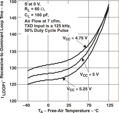 Figure 1. Recessive-to-Dominant Loop Time vs Free-Air Temperature (Across VCC)
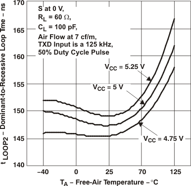 Figure 2. Dominant-to-Recessive Loop Time vs Free-Air Temperature (Across VCC)
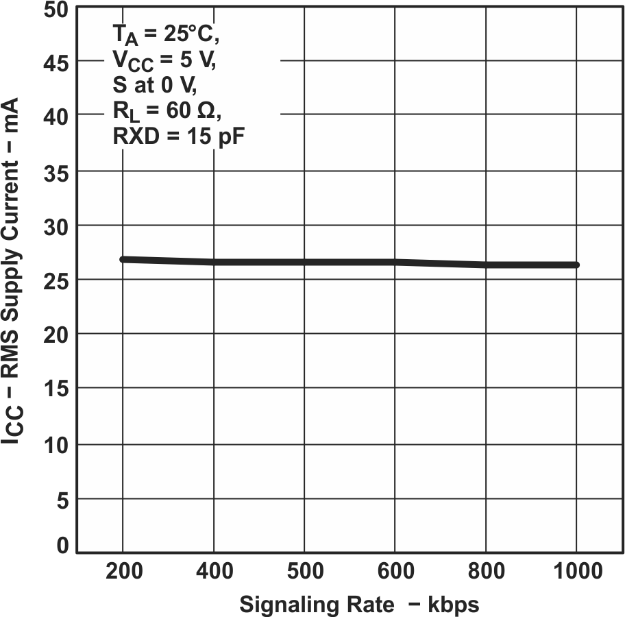 Figure 3. Supply Current (RMS) vs Signaling Rate
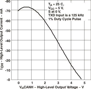 Figure 5. Driver High-Level Output Voltage vs High-Level Output Current
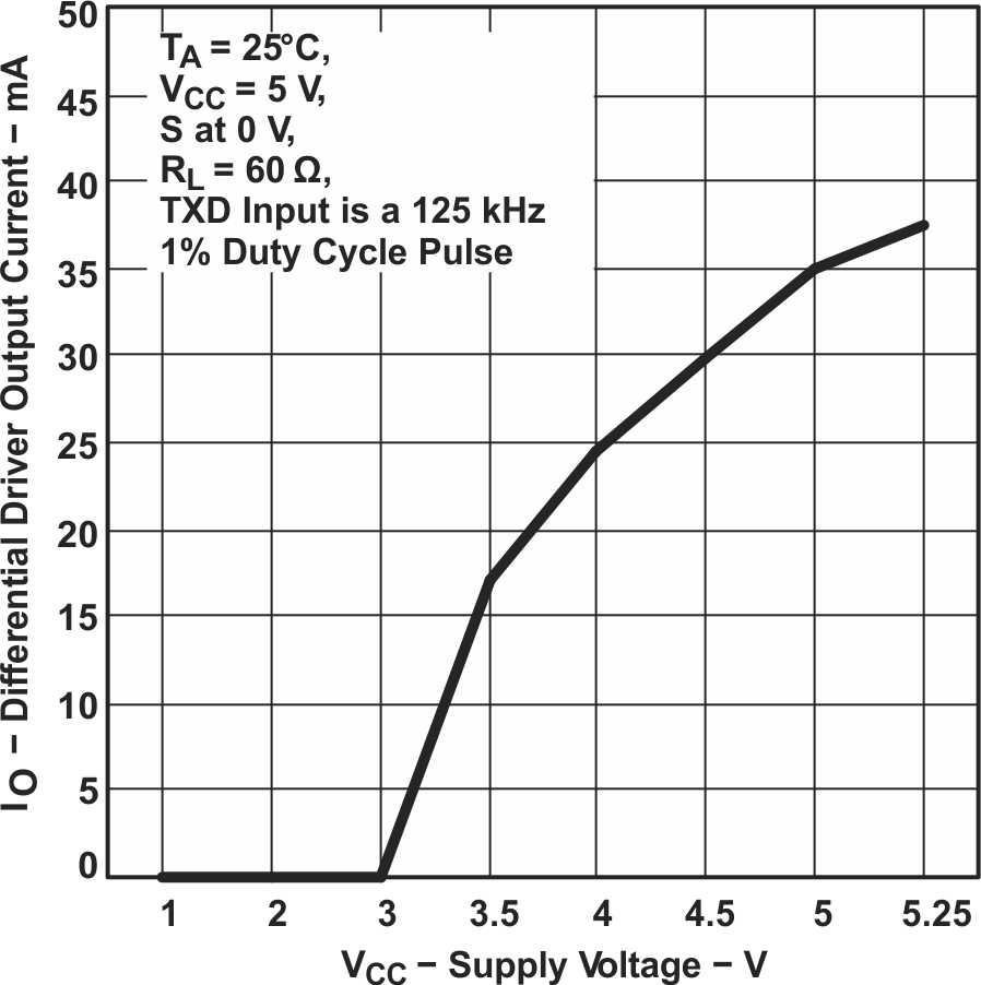 Figure 7. Driver Output Current vs Supply Voltage
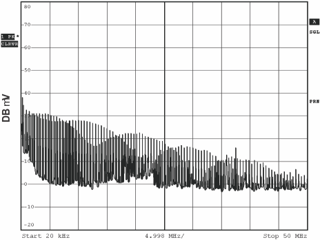 Figure 9. Frequency Spectrum of Common-Mode Emissions
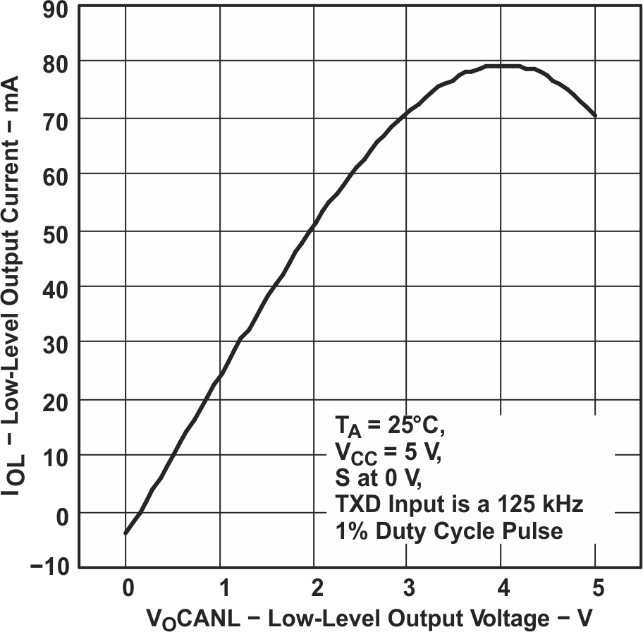 Figure 4. Driver Low-Level Output Voltage vs Low-Level Output Current
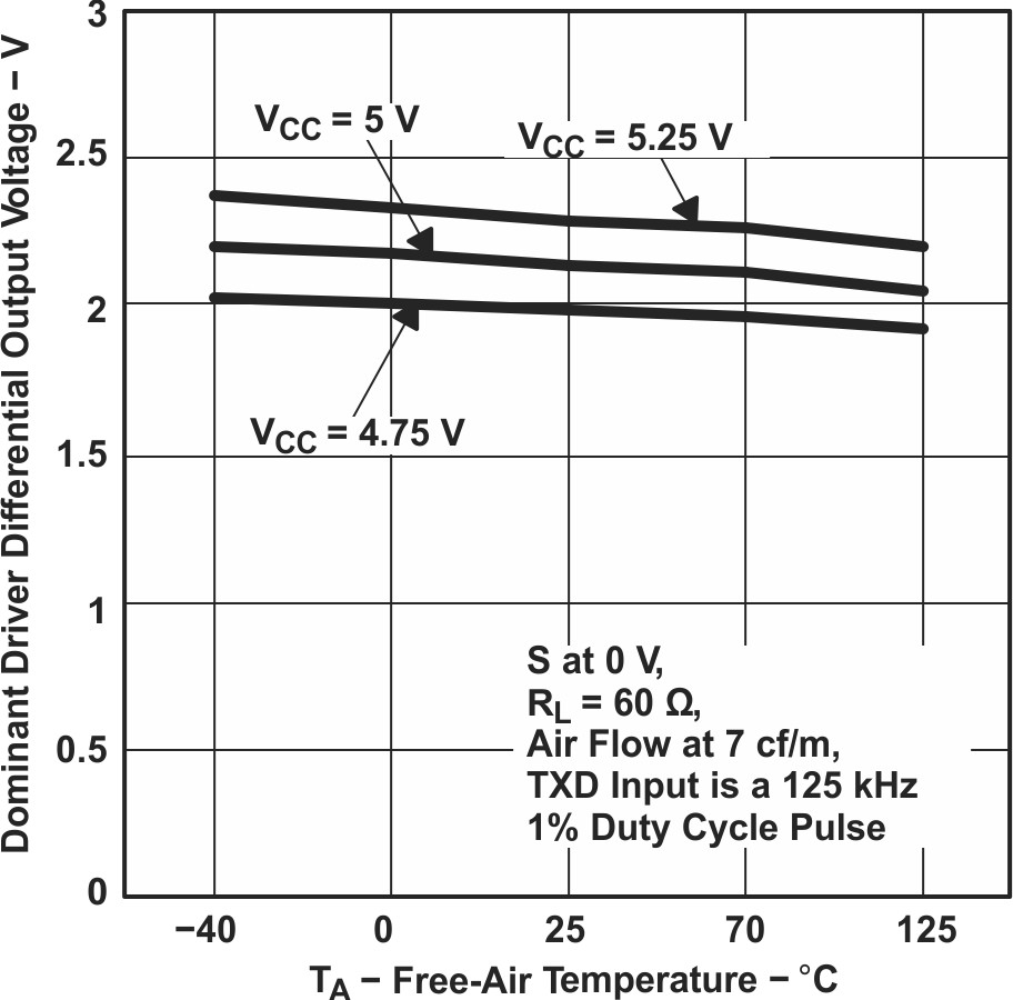 Figure 6. Driver Differential Output Voltage vs Free-Air Temperature (Across VCC)
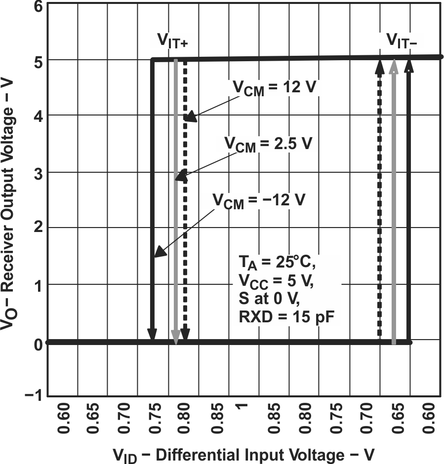 Figure 8. Receiver Output Voltage vs Differential Input Voltage
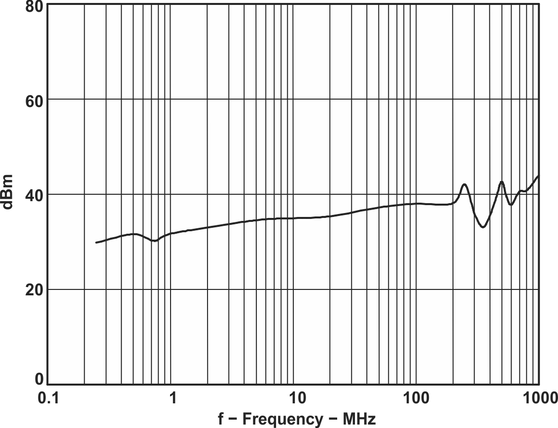 Figure 10. Direct Power Injection (DPI) Response vs Frequency