JAJSH83E June 2014 – April 2019 SN65HVD1470 , SN65HVD1471 , SN65HVD1473 , SN65HVD1474 , SN65HVD1476 , SN65HVD1477
PRODUCTION DATA.
- 1 特長
- 2 アプリケーション
- 3 概要
- 4 改訂履歴
- 5 Device Comparison Table
- 6 Pin Configuration and Functions
-
7 Specifications
- 7.1 Absolute Maximum Ratings
- 7.2 ESD Ratings
- 7.3 Recommended Operating Conditions
- 7.4 Thermal Information — D Packages
- 7.5 Thermal Information — DGS and DGK Packages
- 7.6 Power Dissipation
- 7.7 Electrical Characteristics
- 7.8 Switching Characteristics — 400 kbps
- 7.9 Switching Characteristics — 20 Mbps
- 7.10 Switching Characteristics — 50 Mbps
- 7.11 Typical Characteristics
- 8 Parameter Measurement Information
- 9 Detailed Description
- 10Application and Implementation
- 11Power Supply Recommendations
- 12Layout
- 13デバイスおよびドキュメントのサポート
- 14メカニカル、パッケージ、および注文情報
パッケージ・オプション
メカニカル・データ(パッケージ|ピン)
サーマルパッド・メカニカル・データ
発注情報
8 Parameter Measurement Information
The input generator rate is 100 kbps with 50% duty cycle, than 6-ns rise and fall times, and 50-Ω output impedance.
 Figure 15. Measurement of Driver Differential Output Voltage With Common-Mode Load
  Figure 16. Measurement of Driver Differential and Common-Mode Output With RS-485 Load
  Figure 17. Measurement of Driver Differential Output Rise and Fall Times and Propagation Delays
D at 3 V to test non-inverting output, D at 0 V to test inverting output.
Figure 18. Measurement of Driver Enable and Disable Times with Active-High Output and Pulldown Load 
D at 0 V to test non-inverting output, D at 3 V to test inverting output.
Figure 19. Measurement of Driver Enable and Disable Times with Active-Low Output and Pullup Load  Figure 20. Measurement of Receiver Output Rise and Fall Times and Propagation Delays
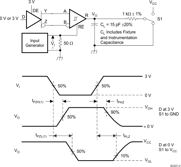
  Figure 21. Measurement of Receiver Enable and Disable Times With Driver Enabled
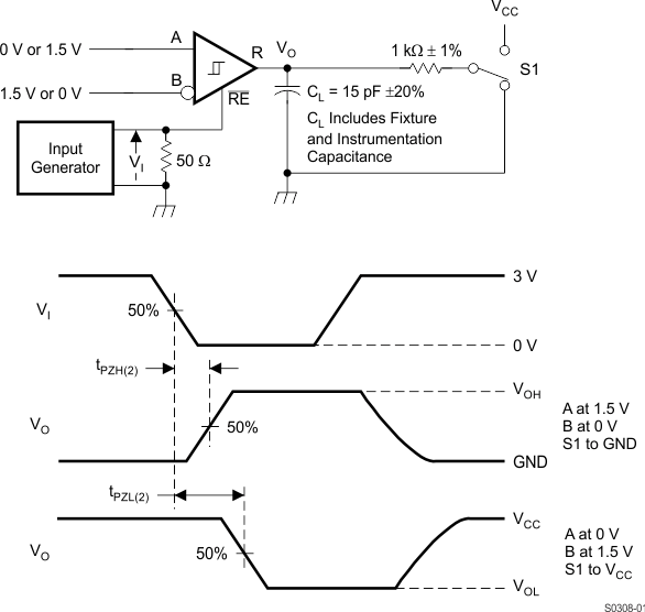
  Figure 22. Measurement of Receiver Enable Times With Driver Disabled