JAJS488J January   2008  – March 2023 SN65HVD1785 , SN65HVD1786 , SN65HVD1787 , SN65HVD1791 , SN65HVD1792 , SN65HVD1793

PRODUCTION DATA  

  1. 特長
  2. アプリケーション
  3. 概要
  4. Revision History
  5. Product Selection Guide
  6. Pin Configuration and Functions
  7. Specifications
    1. 7.1 Absolute Maximum Ratings #GUID-EF6E23B6-467E-4F27-83DC-9566F6730B27/SLLS8725683
    2. 7.2 ESD Ratings
    3. 7.3 Recommended Operating Conditions
    4. 7.4 Thermal Information
    5. 7.5 Electrical Characteristics
    6. 7.6 Thermal Considerations
    7. 7.7 Switching Characteristics
    8. 7.8 Typical Characteristics
  8. Parameter Measurement Information
  9. Detailed Description
    1. 9.1 Overview
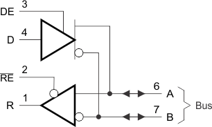
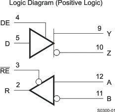
    2. 9.2 Functional Block Diagram
    3. 9.3 Feature Description
      1. 9.3.1 Hot-Plugging
      2. 9.3.2 Receiver Failsafe
      3. 9.3.3 70-V Fault-Protection
      4. 9.3.4 Additional Options
    4. 9.4 Device Functional Modes
  10. 10Application and Implementation
    1. 10.1 Application Information
    2. 10.2 Typical Application
      1. 10.2.1 Design Requirements
        1. 10.2.1.1 Data Rate and Bus Length
        2. 10.2.1.2 Stub Length
        3. 10.2.1.3 Receiver Failsafe
      2. 10.2.2 Detailed Design Procedure
      3. 10.2.3 Application Curve
  11. 11Power Supply Recommendations
  12. 12Layout
    1. 12.1 Layout Guidelines
    2. 12.2 Layout Example
  13. 13Device and Documentation Support
    1. 13.1 Documentation Support
    2. 13.2 ドキュメントの更新通知を受け取る方法
    3. 13.3 サポート・リソース
    4. 13.4 Trademarks
    5. 13.5 静電気放電に関する注意事項
    6. 13.6 用語集
  14. 14Mechanical, Packaging, and Orderable Information

パッケージ・オプション

メカニカル・データ(パッケージ|ピン)
サーマルパッド・メカニカル・データ
発注情報

Functional Block Diagram

GUID-060193C7-1FB2-49D2-9349-2B967DF87C78-low.gif Figure 9-1 Half-Duplex Transceiver
GUID-7DCA5D75-3647-4D14-ADAB-3F6406450052-low.gif Figure 9-2 Full Duplex Transceiver