SN65HVD233-HT 3.3-V CAN Transceiver
1 Features
- Bus-Pin Fault Protection Exceeds ±36 V
- Bus-Pin ESD Protection Exceeds 16-kV Human Body Model (HBM)
- Compatible With ISO 11898
- Signaling Rates(1) up to 1 Mbps
- Extended –7-V to 12-V Common-Mode Range
- High-Input Impedance Allows for 120 Nodes
- LVTTL I/Os Are 5-V Tolerant
- Adjustable Driver Transition Times for Improved Signal Quality
- Unpowered Node Does Not Disturb the Bus
- Low-Current Standby Mode: 200 µA Typical
- Power-Up and Power-Down Glitch-Free Bus Inputs and Outputs
- High-Input Impedance With Low VCC
- Monolithic Output During Power Cycling
- Loopback for Diagnostic Functions Available
- DeviceNet™ Vendor ID #806 (1)
2 Applications
- Down-Hole Drilling
- High-Temperature Environments
- Industrial Automation
- DeviceNet Data Buses
- Smart Distributed Systems (SDS™)
- SAE J1939 Data Bus Interfaces
- NMEA 2000 Data Bus Interfaces
- ISO 11783 Data Bus Interfaces
- CAN Data Bus Interfaces
- Controlled Baseline
- One Assembly or Test Site
- One Fabrication Site
- Available in Extreme (–55°C to 210°C) Temperature Range (1)
- Extended Product Life Cycle
- Extended Product-Change Notification
- Product Traceability
- Texas Instruments high-temperature products use highly optimized silicon (die) solutions with design and process enhancements to maximize performance over extended temperatures.
3 Description
The SN65HVD233 is used in applications employing the controller area network (CAN) serial communication physical layer in accordance with the ISO 11898 standard, with the exception that the thermal shutdown is removed. As a CAN transceiver, the device provides transmit and receive capability between the differential CAN bus and a CAN controller, with signaling rates up to 1 Mbps.
Designed for operation in especially harsh environments, the device features cross wire, overvoltage, and loss-of-ground protection to ±36 V, with common-mode transient protection of ±100 V. This device operates over a –7-V to 12-V common-mode range with a maximum of 60 nodes on a bus.
If the common-mode range is restricted to the ISO 11898 standard range of –2 V to 7 V, up to 120 nodes may be connected on a bus. This transceiver interfaces the single-ended CAN controller with the differential CAN bus found in industrial, building automation, and automotive applications.
Device Information(1)
| PART NUMBER | PACKAGE | BODY SIZE (NOM) |
|---|---|---|
| SN65HVD233-HT | SOIC (8) | 4.90 mm x 3.91 mm |
| CFP-HKJ (8) | 6.90 mm x 5.65 mm | |
| CFP-HKQ (8) | 6.90 mm x 5.65 mm | |
| CDIP SB (8) | 40.64 mm x 10.04 mm |
- For all available packages, see the orderable addendum at the end of the datasheet.
Functional Block Diagram

4 Revision History
Changes from F Revision (August 2012) to G Revision
- Added Handling Rating table, Feature Description section, Device Functional Modes, Application and Implementation section, Power Supply Recommendations section, Layout section, Device and Documentation Support section, and Mechanical, Packaging, and Orderable Information section Go
5 Description (Continued)
RS (pin 8) provides for three modes of operation: high-speed, slope control, or low-power standby mode. The high-speed mode of operation is selected by connecting RS directly to ground, thus allowing the driver output transistors to switch on and off as fast as possible with no limitation on the rise and fall slope. The rise and fall slope can be adjusted by connecting a resistor to ground at RS, because the slope is proportional to the output current of the pin. Slope control is implemented with a resistor value of 10 kΩ to achieve a slew rate of
≉ 15 V/μs, and a value of 100 kΩ to achieve ≉ 2 V/μs slew rate. For more information about slope control, refer to the Application and Implementation section.
The SN65HVD233 enters a low-current standby mode, during which the driver is switched off and the receiver remains active if a high logic level is applied to RS. The local protocol controller reverses this low-current standby mode when it needs to transmit to the bus.
A logic high on the loopback (LBK, pin 5) of the SN65HVD233 places the bus output and bus input in a high-impedance state. The remaining circuit remains active and available for the driver to receiver loopback, self-diagnostic node functions without disturbing the bus.
6 Pin Configuration and Functions


Pin Functions
| PIN | TYPE | DESCRIPTION | |
|---|---|---|---|
| NO. | NAME | ||
| 1 | D | I | CAN Transmit Data input (Low for dominant and HIGH for recessive bus states) |
| 2 | GND | Power | Ground connection |
| 3 | VCC | Power | VCC |
| 4 | R | O | CAN Receive data output |
| 5 | LBK | I | LoopBack (Active high to enable controller loopback mode) |
| 6 | CFANL | I/O | Low level CAN bus line |
| 7 | CANH | I/O | High level CAN bus line |
| 8 | Rs | I | High Speed, Slope control, and standby enable mode input. |
Bare Die Information
| DIE THICKNESS | BACKSIDE FINISH | BACKSIDE POTENTIAL | BOND PAD METALLIZATION COMPOSITION |
|---|---|---|---|
| 15 mils. | Silicon with backgrind | GND | Al-Si-Cu (0.5%) |

Bond Pad Coordinates In Microns - Rev A
| DESCRIPTION | PAD NUMBER | A | B | C | D |
|---|---|---|---|---|---|
| D | 1 | 86.40 | 157.85 | 203.40 | 274.85 |
| GND | 2 | 1035.05 | 69.75 | 1150.05 | 184.75 |
| GND | 3 | 1168.15 | 69.75 | 1283.15 | 184.75 |
| VCC | 4 | 1572.05 | 51.85 | 1687.05 | 166.85 |
| VCC | 5 | 1711.95 | 51.85 | 1826.95 | 166.85 |
| R | 6 | 2758.85 | 237.65 | 2873.85 | 352.65 |
| LBK | 7 | 2774.25 | 1429.985 | 2889.25 | 1544.95 |
| CANL | 8 | 1549.90 | 1544.95 | 1664.90 | 1659.95 |
| CANH | 9 | 1351.45 | 1544.95 | 1466.45 | 1659.95 |
| RS | 10 | 83.50 | 1429.95 | 198.50 | 1544.95 |

7 Specifications
7.1 Absolute Maximum Ratings
over operating free-air temperature range (unless otherwise noted) (1)(2)| MIN | MAX | UNIT | ||
|---|---|---|---|---|
| VCC | Supply voltage range | –0.3 | 7 | V |
| Voltage range at any bus terminal (CANH or CANL) | –36 | 36 | V | |
| Voltage input range, transient pulse (CANH and CANL) through 100 Ω (see Figure 19) | –100 | 100 | V | |
| VI | Input voltage range (D, R, RS, LBK) | –0.5 | 7 | V |
| IO | Receiver output current | –10 | 10 | mA |
| Tstg | Storage temperature | –65 | 150 | °C |
7.2 ESD Ratings
| VALUE | UNIT | |||||
|---|---|---|---|---|---|---|
| V(ESD) | Electrostatic discharge | Human body model (HBM), per ANSI/ESDA/JEDEC JS-001, all pins(1) | CANH, CANL, and GND | ±16000 | V | |
| All pins | ±3000 | |||||
| Charged device model (CDM), per JEDEC specification JESD22-C101, all pins(2) | ±1000 | |||||
7.3 Recommended Operating Conditions
TA = –55°C to 210°C| MIN | MAX | UNIT | |||
|---|---|---|---|---|---|
| VCC | Supply voltage | 3 | 3.6 | V | |
| Voltage at any bus terminal (separately or common mode) | –7 | 12 | V | ||
| VIH | High-level input voltage | D, LBK | 2 | 5.5 | V |
| VIL | Low-level input voltage | D, LBK | 0 | 0.8 | V |
| VID | Differential input voltage | –6 | 6 | V | |
| Resistance from RS to ground | 0 | 100 | kΩ | ||
| VI(Rs) | Input voltage at RS for standby | 0.75 VCC | 5.5 | V | |
| IOH | High-level output current | Driver | –50 | mA | |
| Receiver | –10 | ||||
| IOL | Low-level output current | Driver | 50 | mA | |
| Receiver | 10 | ||||
| TJ | Operating junction temperature | 212 | °C | ||
| TA | Operating free-air temperature(1) | –55 | 210 | °C | |
7.4 Thermal Information
| THERMAL METRIC(1) | SN65HVD233-HT | UNIT | |||
|---|---|---|---|---|---|
| D | HJK/HKQ | JDJ | |||
| 8 PINS | 8 PINS | 8 PINS | |||
| RθJA | Junction-to-ambient thermal resistance | 106.4 | 146.1 | 72.7 | °C/W |
| RθJC(top) | Junction-to-case (top) thermal resistance | 55.8 | 23.7 | 3.1 | |
| RθJB | Junction-to-board thermal resistance | 46.5 | 152.0 | 38.3 | |
| ψJT | Junction-to-top characterization parameter | 10.7 | 20.7 | 6.0 | |
| ψJB | Junction-to-board characterization parameter | 45.9 | 93.1 | 26.9 | |
7.5 Driver Electrical Characteristics
over operating free-air temperature range (unless otherwise noted)| PARAMETER | TEST CONDITIONS | TA = –55°C to 125°C | TA = 175°C(1) | TA = 210°C(2) | UNIT | |||||||||
|---|---|---|---|---|---|---|---|---|---|---|---|---|---|---|
| MIN | TYP | MAX | MIN | TYP | MAX | MIN | TYP | MAX | ||||||
| VO(D) | Bus output voltage (dominant) |
CANH | D = 0 V, RS = 0 V, See Figure 13 and Figure 14 |
2.45 | VCC | 2.45 | VCC | 2.45 | VCC | V | ||||
| CANL | 0.5 | 1.25 | 0.5 | 1.25 | 0.5 | 1.25 | ||||||||
| VO | Bus output voltage (recessive) | CANH | D = 3 V, RS = 0 V, See Figure 13 and Figure 14 |
2.3 | 2.3 | 2.3 | V | |||||||
| CANL | 2.3 | 2.3 | 2.3 | |||||||||||
| VOD(D) | Differential output voltage (Dominant) | D = 0 V, RS = 0 V, See Figure 13 and Figure 14 |
1.5 | 2 | 3 | 1.4 | 1.75 | 3 | 1.4 | 1.75 | 3 | V | ||
| D = 0 V, RS = 0 V, See Figure 14 and Figure 15 |
1.1 | 2 | 3 | 1.1 | 1.47 | 3 | 1.1 | 1.47 | 3 | |||||
| VOD | Differential output voltage (Recessive) | D = 3 V, RS = 0 V, See Figure 13 and Figure 14 |
–120 | 12 | –120 | 12 | –120 | 12 | mV | |||||
| D = 3 V, RS = 0 V, No load | –0.5 | 0.05 | –0.5 | 0.8 | –0.5 | 1.2 | V | |||||||
| VOC(pp) | Peak-to-peak common-mode output voltage | See Figure 21 | 1 | 1 | 1 | V | ||||||||
| IIH | High-level input current | D, LBK | D = 2 V | –30 | 30 | –30 | 30 | –30 | 30 | μA | ||||
| IIL | Low-level input current | D, LBK | D = 0.8 V | –30 | 30 | –30 | 30 | –30 | 30 | μA | ||||
| IOS | Short-circuit output current | VCANH = –7 V, CANL open, See Figure 24 |
–250 | –250 | –250 | mA | ||||||||
| VCANH = 12 V, CANL open, See Figure 24 |
1 | 1 | 1 | |||||||||||
| VCANL = –7 V, CANH open, See Figure 24 |
–1 | –1 | –1 | |||||||||||
| VCANL = 12 V, CANH open, See Figure 24 |
250 | 250 | 250 | |||||||||||
| CO | Output capacitance | See receiver input capacitance | ||||||||||||
| IIRs(s) | RS input current for standby | RS = 0.75 VCC | –10 | –10 | –10 | μA | ||||||||
| ICC | Supply current | Standby | RS = VCC, D = VCC, LBK = 0 V |
200 | 600 | 400 | 600 | 400 | 600 | μA | ||||
| Dominant | D = 0 V, No load, LBK = 0 V, RS = 0 V |
6 | 6 | 6 | mA | |||||||||
| Recessive | D =t VCC, No load, LBK = 0 V, RS = 0 V |
6 | 6 | 6 | ||||||||||
7.6 Receiver Electrical Characteristics
over operating free-air temperature range (unless otherwise noted)| PARAMETER | TEST CONDITIONS | TA = –55°C to 125°C | TA = 175°C(1) | TA = 210°C(2) | UNIT | |||||||||
|---|---|---|---|---|---|---|---|---|---|---|---|---|---|---|
| MIN | TYP | MAX | MIN | TYP | MAX | MIN | TYP | MAX | ||||||
| VIT+ | Positive-going input threshold voltage | LBK = 0 V, See Table 1 | 620 | 900 | 600 | 900 | 600 | 900 | mV | |||||
| VIT– | Negative-going input threshold voltage | 500 | 715 | 500 | 725 | 500 | 725 | mV | ||||||
| Vhys | Hysteresis voltage (VIT+ – VIT–) |
100 | 140 | 140 | mV | |||||||||
| VOH | High-level output voltage | IO = –4 mA, See Figure 18 | 2.4 | 2.4 | 2.4 | V | ||||||||
| VOL | Low-level output voltage | IO = 4 mA, See Figure 18 | 0.4 | 0.4 | 0.4 | V | ||||||||
| II | Bus input current | CANH or CANL = 12 V |
Other bus pin = 0 V, D = 3 V, LBK = 0 V, RS = 0 V, |
140 | 500 | 140 | 500 | 140 | 500 | μA | ||||
| CANH or CANL = 12 V, VCC = 0 V |
200 | 600 | 200 | 700 | 200 | 800 | ||||||||
| CANH or CANL = –7 V |
–610 | –150 | –610 | –150 | –610 | –150 | ||||||||
| CANH or CANL = –7 V, VCC = 0 V |
–450 | –130 | –450 | –130 | –450 | –130 | ||||||||
| CI | Input capacitance (CANH or CANL) |
Pin to ground, VI = 0.4 sin (4E6πt) + 0.5 V, D = 3 V, LBK = 0 V |
45 | 55 | 55 | pF | ||||||||
| CID | Differential input capacitance | Pin to pin, VI = 0.4 sin (4E6πt) + 0.5 V, D = 3 V, LBK = 0 V |
15 | 15 | 15 | pF | ||||||||
| RID | Differential input resistance | D = 3 V, LBK = 0 V | 40 | 110 | 40 | 110 | 40 | 110 | kΩ | |||||
| RIN | Input resistance (CANH or CANL) |
20 | 51 | 19 | 51 | 18 | 51 | kΩ | ||||||
| ICC | Supply current | Standby | RS = VCC, D = VCC, LBK = 0 V | 200 | 600 | 400 | 600 | 400 | 600 | μA | ||||
| Dominant | D = 0 V, No load, RS = 0 V, LBK = 0 V |
6 | 6 | 6 | mA | |||||||||
| Recessive | D = VCC, No load, RS = 0 V, LBK = 0 V |
6 | 6 | 6 | ||||||||||
TA = 175°C.
7.7 Driver Switching Characteristics
over operating free-air temperature range (unless otherwise noted)| PARAMETER | TEST CONDITIONS | TA = –55°C to 125°C | TA = 175°C(1) | TA = 210°C(2) | UNIT | |||||||
|---|---|---|---|---|---|---|---|---|---|---|---|---|
| MIN | TYP | MAX | MIN | TYP | MAX | MIN | TYP | MAX | ||||
| tPLH | Propagation delay time, low-to-high-level output |
RS = 0 V, See Figure 16 | 35 | 85 | 50 | 50 | ns | |||||
| RS with 10 kΩ to ground, See Figure 16 |
70 | 125 | 75 | 75 | ||||||||
| RS with 100 kΩ to ground, See Figure 16 |
500 | 870 | 500 | 500 | ||||||||
| tPHL | Propagation delay time, high-to-low-level output |
RS = 0 V, See Figure 16 |
70 | 120 | 70 | 70 | ns | |||||
| RS with 10 kΩ to ground, See Figure 16 |
130 | 180 | 130 | 130 | ||||||||
| RS with 100 kΩ to ground, See Figure 16 |
870 | 1200 | 870 | 870 | ||||||||
| tsk(p) | Pulse skew (|tPHL – tPLH|) |
RS = 0 V, See Figure 16 |
35 | 9 | 9 | ns | ||||||
| RS with 10 kΩ to ground, See Figure 16 |
60 | 35 | 35 | |||||||||
| RS with 100 kΩ to ground, See Figure 16 |
370 | 475 | 475 | |||||||||
| tr | Differential output signal rise time | RS = 0 V, See Figure 16 | 20 | 70 | 20 | 75 | 20 | 75 | ns | |||
| tf | Differential output signal fall time | 18 | 70 | 20 | 75 | 20 | 75 | |||||
| tr | Differential output signal rise time | RS with 10 kΩ to ground, See Figure 16 |
30 | 135 | 30 | 140 | 30 | 140 | ns | |||
| tf | Differential output signal fall time | 30 | 135 | 30 | 140 | 30 | 140 | |||||
| tr | Differential output signal rise time | RS with 100 kΩ to ground, See Figure 16 |
250 | 1400 | 250 | 1400 | 250 | 1400 | ns | |||
| tf | Differential output signal fall time | 350 | 1400 | 350 | 1400 | 350 | 1400 | |||||
| ten(s) | Enable time from standby to dominant | See Figure 20 | 0.6 | 1.5 | 0.6 | 1.5 | 0.6 | 1.5 | μs | |||
7.8 Receiver Switching Characteristics
over operating free-air temperature range (unless otherwise noted)| PARAMETER | TEST CONDITIONS | TA = –55°C to 125°C | TA = 175°C(1) | TA = 210°C(2) | UNIT | |||||||
|---|---|---|---|---|---|---|---|---|---|---|---|---|
| MIN | TYP | MAX | MIN | TYP | MAX | MIN | TYP | MAX | ||||
| tPLH | Propagation delay time, low-to-high-level output | See Figure 18 | 35 | 60 | 50 | 60 | 50 | 60 | ns | |||
| tPHL | Propagation delay time, high-to-low-level output | 35 | 60 | 45 | 60 | 45 | 60 | ns | ||||
| tsk(p) | Pulse skew (|tPHL – tPLH|) | 7 | 5 | 5 | ns | |||||||
| tr | Output signal rise time | 2 | 6.5 | 6.5 | 8 | 6.5 | 8 | ns | ||||
| tf | Output signal fall time | 2 | 6.5 | 6.5 | 9 | 6.5 | 9 | ns | ||||
7.9 Device Switching Characteristics
over operating free-air temperature range (unless otherwise noted)| PARAMETER | TEST CONDITIONS | TA = –55°C to 125°C | TA = 175°C(1) | TA = 210°C(2) | UNIT | ||||||||
|---|---|---|---|---|---|---|---|---|---|---|---|---|---|
| MIN | TYP | MAX | MIN | TYP | MAX | MIN | TYP | MAX | |||||
| t(LBK) | Loopback delay, driver input to receiver output | See Figure 23 | 7.5 | 15 | 12 | 15 | 12 | 15 | ns | ||||
| t(loop1) | Total loop delay, driver input to receiver output, recessive to dominant | RS = 0 V, See Figure 22 | 70 | 135 | 90 | 135 | 90 | 135 | ns | ||||
| RS with 10 kΩ to ground, See Figure 22 |
105 | 190 | 115 | 190 | 115 | 190 | |||||||
| RS with 100 kΩ to ground, See Figure 22 |
535 | 1000 | 430 | 1000 | 430 | 1000 | |||||||
| t(loop2) | Total loop delay, driver input to receiver output, dominant to recessive | RS = 0 V, See Figure 22 | 70 | 135 | 98 | 135 | 98 | 135 | ns | ||||
| RS with 10 kΩ to ground, See Figure 22 |
105 | 190 | 150 | 190 | 150 | 190 | |||||||
| RS with 100 kΩ to ground, See Figure 22 |
535 | 1100 | 880 | 1200 | 880 | 1200 | |||||||

SN65HVD233HD, SN65HVD233SJD, SN65HVD233SKGDA, SN65HVD233SHKJ, SN65HVD233SHKQ
7.10 Typical Characteristics


vs Free-Air Temperature


vs Free-Air Temperature
8 Parameter Measurement Information
 Figure 13. Driver Voltage, Current, and Test Definition
 Figure 14. Bus Logic State Voltage Definitions
 Figure 15. Driver VOD

 Figure 17. Receiver Voltage and Current Definitions

Table 1. Differential Input Voltage Threshold Test
| INPUT | OUTPUT | MEASURED | ||
|---|---|---|---|---|
| VCANH | VCANL | R | |VID| | |
| –6.1 V | –7 V | L | VOL | 900 mV |
| 12 V | 11.1 V | L | 900 mV | |
| –1 V | –7 V | L | 6 V | |
| 12 V | 6 V | L | 6 V | |
| –6.5 V | –7 V | H | VOH | 500 mV |
| 12 V | 11.5 V | H | 500 mV | |
| –7 V | –1 V | H | 6 V | |
| 6 V | 12 V | H | 6 V | |
| Open | Open | H | X | |

 Figure 20. Ten(s) Test Circuit and Voltage Waveforms
 Figure 21. VOC(pp) Test Circuit and Voltage Waveforms
 Figure 22. T(loop) Test Circuit and Voltage Waveforms
 Figure 23. T(LBK) Test Circuit and Voltage Waveforms
 Figure 24. IOS Test Circuit and Waveforms

9 Detailed Description
9.1 Overview
Controller Area Network (CAN) is a robust multi master-master, differential signaling, serial communications bus specified by the ISO 11898 family of standards. TI's SSN65HVD23x family of transceivers solve specialized networking requirements for various applications.
Table 2. Available Options
| ORDERABLE PART NUMBER | LOW-POWER MODE | SLOPE CONTROL |
DIAGNOSTIC LOOPBACK |
AUTOBAUD LOOPBACK |
|---|---|---|---|---|
| SN65HVD233HD | 200-μA standby mode | Adjustable | Yes | No |
| SN65HVD233SJD | ||||
| SN65HVD233SKGDA | ||||
| SN65HVD233SHKJ | ||||
| SN65HVD233SHKQ |
9.2 Functional Block Diagram
9.3 Feature Description
9.3.1 ISO 11898 Compliance of SN65HVD23x Family of 3.3-V CAN Transceivers
Many users value the low power consumption of operating CAN transceivers from a 3.3-V supply. However, some are concerned about the interoperability with 5-V supplied transceivers on the same bus. This section analyzes this situation to address those concerns.
9.3.1.1 Differential Signal
CAN is a differential bus where complementary signals are sent over two wires, and the voltage difference between the two wires defines the logical state of the bus. The differential CAN receiver monitors this voltage difference and outputs the bus state with a single-ended output signal.
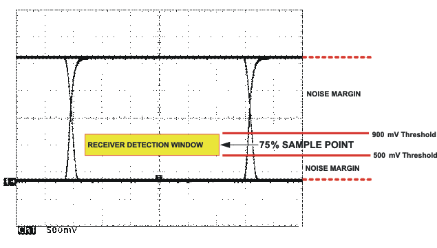 Figure 26. Typical SN65HVD23x Differential Output Voltage Waveform
The CAN driver creates the difference voltage between CANH and CANL in the dominant state. The dominant differential output of the SN65HVD23x is greater than 1.5 V and less than 3 V across a 60-Ω load. The minimum required by ISO 11898 is 1.5 V and the maximum is 3 V. These are the same limiting values for 5-V supplied CAN transceivers. The bus termination resistors drive the recessive bus state and not the CAN driver.
A CAN receiver is required to output a recessive state with less than 500 mV and a dominant state with more than 900-mV difference voltage on its bus inputs. The CAN receiver must do this with common-mode input voltages from –2 V to 7 V. The SN65HVD23x family receivers meet these same input specifications as 5-V supplied receivers.
9.3.1.1.1 Common-Mode Signal
A common-mode signal is an average voltage of the two signal wires that the differential receiver rejects. The common-mode signal comes from the CAN driver, ground noise, and coupled bus noise. Obviously, the supply voltage of the CAN transceiver has nothing to do with noise. The SN65HVD23x family driver lowers the common-mode output in a dominant bit by a couple hundred millivolts from that of most 5-V drivers. While this does not fully comply with ISO 11898, this small variation in the driver common-mode output is rejected by differential receivers and does not affect data, signal noise margins, or error rates.
9.3.1.2 Interoperability Of 3.3-V CAN in 5-V CAN Systems
The 3.3-V–supplied SN65HVD23x family of CAN transceivers are electrically interchangeable with 5-V CAN transceivers. The differential output is the same. The recessive common-mode output is the same. The dominant common-mode output voltage is a couple hundred millivolts lower than 5-V–supplied drivers, while the receivers exhibit identical specifications as 5-V devices.
Electrical interoperability does not assure interchangeability however. Most implementers of CAN buses recognize that ISO 11898 does not sufficiently specify the electrical layer and that strict standard compliance alone does not ensure interchangeability. This comes only with thorough equipment testing.
9.4 Device Functional Modes
9.4.1 Function Tables
Table 3. Function Table (Driver)(1)
| DRIVER | |||||
|---|---|---|---|---|---|
| INPUTS | OUTPUTS | ||||
| D | LBK | Rs | CANH | CANL | BUS STATE |
| X | X | >0.75 VCC | Z | Z | Recessive |
| L | L or open | ≤0.33 VCC | H | L | Dominant |
| H or open | X | Z | Z | Recessive | |
| X | H | ≤0.33 VCC | Z | Z | Recessive |
Table 4. Function Table (Receiver)
| RECEIVER | ||||
|---|---|---|---|---|
| INPUTS | OUTPUT | |||
| BUS STATE | VID = V(CANH) – V(CANL) | LBK | D | R |
| Dominant | VID ≥ 0.9 V | L or open | X | L |
| Recessive | VID ≤ 0.5 V or open | L or open | H or open | H |
| ? | 0.5 V < VID < 0.9 V | L or open | H or open | |
| X | X | H | L | L |
| X | X | H | H | |
9.4.2 Equivalent Input and Output Schematic Diagrams
 Figure 27. D Input
 Figure 29. CANH Input
 Figure 31. CANH and CANL Outputs
 Figure 33. LBK Input
 Figure 28. RS Input
 Figure 30. CANL Input
 Figure 32. R Output