JAJSGJ1H November 2002 – November 2018 SN65HVD233 , SN65HVD234 , SN65HVD235
PRODUCTION DATA.
- 1 特長
- 2 アプリケーション
- 3 概要
- 4 改訂履歴
- 5 概要(続き)
- 6 Device Comparison Table
- 7 Pin Configuration and Functions
-
8 Specifications
- 8.1 Absolute Maximum Ratings
- 8.2 ESD Ratings
- 8.3 Recommended Operating Conditions
- 8.4 Thermal Information
- 8.5 Power Dissipation Ratings
- 8.6 Electrical Characteristics: Driver
- 8.7 Electrical Characteristics: Receiver
- 8.8 Switching Characteristics: Driver
- 8.9 Switching Characteristics: Receiver
- 8.10 Switching Characteristics: Device
- 8.11 Typical Characteristics
- 9 Parameter Measurement Information
- 10Detailed Description
- 11Application and Implementation
- 12Power Supply Recommendations
- 13Layout
- 14デバイスおよびドキュメントのサポート
- 15メカニカル、パッケージ、および注文情報
パッケージ・オプション
デバイスごとのパッケージ図は、PDF版データシートをご参照ください。
メカニカル・データ(パッケージ|ピン)
- D|8
サーマルパッド・メカニカル・データ
発注情報
10.3.3 Slope Control
The rise and fall slope of the SN65HVD233, SN65HVD234, and SN65HVD235 driver output can be adjusted by connecting a resistor from the Rs (pin 8) to ground (GND), or to a low-level input voltage as shown in Figure 32.
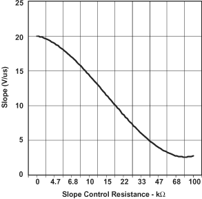
The slope of the driver output signal is proportional to the pin's output current. This slope control is implemented with an external resistor value of 10 kΩ to achieve a ~15 V/μs slew rate, and up to 100 kΩ to achieve a ~2.0 V/μs slew rate . A typical slew rate verses pulldown resistance graph is shown in Figure 33. Typical driver output waveforms with slope control are displayed in Figure 39.
 Figure 32. Slope Control/Standby Connection to a DSP
  Figure 33. HVD233 Driver Output Signal Slope vs Slope Control Resistance Value