JAJSGJ1H November 2002 – November 2018 SN65HVD233 , SN65HVD234 , SN65HVD235
PRODUCTION DATA.
- 1 特長
- 2 アプリケーション
- 3 概要
- 4 改訂履歴
- 5 概要(続き)
- 6 Device Comparison Table
- 7 Pin Configuration and Functions
-
8 Specifications
- 8.1 Absolute Maximum Ratings
- 8.2 ESD Ratings
- 8.3 Recommended Operating Conditions
- 8.4 Thermal Information
- 8.5 Power Dissipation Ratings
- 8.6 Electrical Characteristics: Driver
- 8.7 Electrical Characteristics: Receiver
- 8.8 Switching Characteristics: Driver
- 8.9 Switching Characteristics: Receiver
- 8.10 Switching Characteristics: Device
- 8.11 Typical Characteristics
- 9 Parameter Measurement Information
- 10Detailed Description
- 11Application and Implementation
- 12Power Supply Recommendations
- 13Layout
- 14デバイスおよびドキュメントのサポート
- 15メカニカル、パッケージ、および注文情報
パッケージ・オプション
デバイスごとのパッケージ図は、PDF版データシートをご参照ください。
メカニカル・データ(パッケージ|ピン)
- D|8
サーマルパッド・メカニカル・データ
発注情報
11.2.2 Detailed Design Procedure
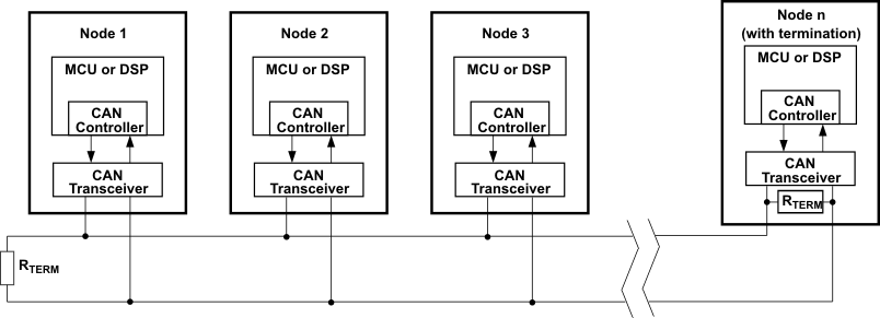
 Figure 37. Typical CAN Bus
 Termination is typically a 120-Ω resistor at each end of the bus. If filtering and stabilization of the common mode voltage of the bus is desired, then split termination may be used (see Figure 38). Split termination uses two 60-Ω resistors with a capacitor in the middle of these resistors to ground. Split termination improves the electromagnetic emissions behavior of the network by eliminating fluctuations in the bus common mode voltages at the start and end of message transmissions.
Care should be taken in the power ratings of the termination resistors used. Typically the worst case condition would be if the system power supply was shorted across the termination resistance to ground. In most cases the current flow through the resistor in this condition would be much higher than the transceiver's current limit.
 Figure 38. CAN Bus Termination Concepts