JAJSPU9M september 2005 – february 2023 SN65HVD30 , SN65HVD31 , SN65HVD32 , SN65HVD33 , SN65HVD34 , SN65HVD35
PRODUCTION DATA
- 1 特長
- 2 アプリケーション
- 3 概要
- 4 Revision History
- 5 Device Comparison
- 6 Pin Configuration and Functions
-
7 Specifications
- 7.1 Absolute Maximum Ratings
- 7.2 ESD Ratings
- 7.3 Recommended Operating Conditions
- 7.4 Thermal Information
- 7.5 Electrical Characteristics: Driver
- 7.6 Electrical Characteristics: Receiver
- 7.7 Device Power Dissipation – PD
- 7.8 Supply Current Characteristics
- 7.9 Switching Characteristics: Driver
- 7.10 Switching Characteristics: Receiver
- 7.11 Dissipation Ratings
- 7.12 Typical Characteristics
- 8 Detailed Description
- 9 Application and Implementation
- 10Device and Documentation Support
- 11Mechanical, Packaging, and Orderable Information
7.12 Typical Characteristics
 Figure 7-1 SN65HVD30, SN65HVD33 RMS Supply Current vs Signaling Rate
 Figure 7-3 SN65HVD32, SN65HVD35 RMS Supply Current vs Signaling Rate
 Figure 7-2 SN65HVD31, SN65HVD34 RMS Supply Current vs Signaling Rate
 Figure 7-4 SN65HVD30, SN65HVD33 Bus Input Current vs Input Voltage
 Figure 7-5 SN65HVD31, SN65HVD32, SN65HVD34, SN65HVD35 Bus Input Current vs Input Voltage
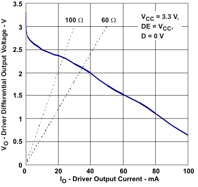
 Figure 7-7 Driver Differential Output Voltage vs Driver Output Current
 Figure 7-9 Driver Output Current vs Supply Voltage
 Figure 7-11 SN65HVD30, SN65HVD33 Driver Rise and Fall Time vs Free-Air Temperature
 Figure 7-13 Receiver Threshold vs Common-Mode Voltage
 Figure 7-15 Enable Time vs Common-Mode Voltage (see Figure 8-1)
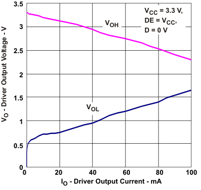
 Figure 7-6 Driver Output Voltage vs Driver Output Current
 Figure 7-8 Driver Differential Output Voltage vs Free-Air Temperature
 Figure 7-10 SN65HVD30, SN65HVD33 Driver Propagation Delay vs Free-Air Temperature
 Figure 7-12 Receiver Threshold vs Ambient Temperature
 Figure 7-14 Supply Current vs Free-Air Temperature