JAJSPU9M september 2005 – february 2023 SN65HVD30 , SN65HVD31 , SN65HVD32 , SN65HVD33 , SN65HVD34 , SN65HVD35
PRODUCTION DATA
- 1 特長
- 2 アプリケーション
- 3 概要
- 4 Revision History
- 5 Device Comparison
- 6 Pin Configuration and Functions
-
7 Specifications
- 7.1 Absolute Maximum Ratings
- 7.2 ESD Ratings
- 7.3 Recommended Operating Conditions
- 7.4 Thermal Information
- 7.5 Electrical Characteristics: Driver
- 7.6 Electrical Characteristics: Receiver
- 7.7 Device Power Dissipation – PD
- 7.8 Supply Current Characteristics
- 7.9 Switching Characteristics: Driver
- 7.10 Switching Characteristics: Receiver
- 7.11 Dissipation Ratings
- 7.12 Typical Characteristics
- 8 Detailed Description
- 9 Application and Implementation
- 10Device and Documentation Support
- 11Mechanical, Packaging, and Orderable Information
パッケージ・オプション
メカニカル・データ(パッケージ|ピン)
サーマルパッド・メカニカル・データ
- RHL|20
発注情報
8.3.4 Receiver Failsafe
The differential receivers of the SN65HVD3x family are failsafe to invalid bus states caused by:
- Open bus conditions such as a disconnected connector
- Shorted bus conditions such as cable damage shorting the twisted-pair together
- Idle bus conditions that occur when no driver on the bus is actively driving
In any of these cases, the differential receiver outputs a failsafe logic high state so that the output of the receiver is not indeterminate.
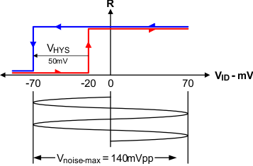
Receiver failsafe is accomplished by offsetting the receiver thresholds such that the input indeterminate range does not include zero volts differential. In order to comply with the RS-422 and RS-485 standards, the receiver output must output a high when the differential input VID is more positive than 200 mV, and must output a low when VID is more negative than –200 mV. The receiver parameters which determine the failsafe performance are VIT+, VIT–, and VHYS (the separation between VIT+ and VIT–. As shown in the Electrical Characteristics table, differential signals more negative than –200 mV always cause a low receiver output, and differential signals more positive than 200 mV always cause a high receiver output.
When the differential input signal is close to zero, it is still above the VIT+ threshold, and the receiver output is high. Only when the differential input is more than VHYS below VIT+ does the receiver output transition to a low state. Therefore, the noise immunity of the receiver inputs during a bus fault conditions includes the receiver hysteresis value (VHYS) as well as the value of VIT+.
 Figure 8-2 SN65HVD30-35 Noise Immunity Under Bus Fault Conditions