SLLSEO3 July 2015 SN65HVD63
PRODUCTION DATA.
- 1 Features
- 2 Applications
- 3 Description
- 4 Revision History
- 5 Device Comparison Table
- 6 Pin Configuration and Functions
- 7 Specifications
- 8 Parameter Measurement Information
- 9 Detailed Description
- 10Application and Implementation
- 11Power Supply Recommendations
- 12Layout
- 13Device and Documentation Support
- 14Mechanical, Packaging, and Orderable Information
パッケージ・オプション
メカニカル・データ(パッケージ|ピン)
- RGT|16
サーマルパッド・メカニカル・データ
- RGT|16
発注情報
12 Layout
12.1 Layout Guidelines
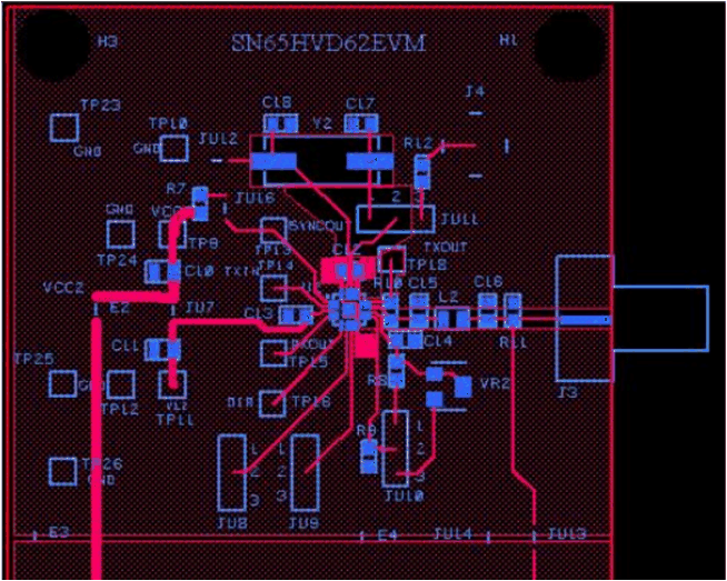
Best practices for high-speed PCB design should be observed because the coax interface to the SN65HVD63 device operates at RF. The RF signaling traces should have a controlled characteristic impedance that is well-matched to the coaxial line. A continuous reference plane should be used to avoid impedance discontinuities. Power and ground distribution should be done through planes rather than traces to decrease series resistance and increase the effective decoupling capacitance on the power rails.
12.2 Layout Example
 Figure 27. SN65HVD63 Layout