SLLS396G SEPTEMBER 1999 – December 2015 SN65LVDS104 , SN65LVDS105
PRODUCTION DATA.
- 1 Features
- 2 Applications
- 3 Description
- 4 Revision History
- 5 Selection Guide to LVDS Repeaters
- 6 Pin Configuration and Functions
-
7 Specifications
- 7.1 Absolute Maximum Ratings
- 7.2 ESD Ratings—JEDEC
- 7.3 ESD Ratings—MIL-STD
- 7.4 Recommended Operating Conditions
- 7.5 Thermal Information
- 7.6 SN65LVDS104 Electrical Characteristics
- 7.7 SN65LVDS105 Electrical Characteristics
- 7.8 SN65LVDS104 Switching Characteristics
- 7.9 SN65LVDS105 Switching Characteristics
- 7.10 Dissipation Ratings
- 7.11 Typical Characteristics
- 8 Parameter Measurement Information
- 9 Detailed Description
-
10Application and Implementation
- 10.1 Application Information
- 10.2
Typical Application
- 10.2.1 Point-to-Point Communications
- 10.2.2 Design Requirements
- 10.2.3
Detailed Design Procedure
- 10.2.3.1 Bypass Capacitance
- 10.2.3.2 Driver Supply Voltage
- 10.2.3.3 Driver Input Voltage
- 10.2.3.4 Driver Output Voltage
- 10.2.3.5 Interconnecting Media
- 10.2.3.6 PCB Transmission Lines
- 10.2.3.7 Termination Resistor
- 10.2.3.8 Receiver Supply Voltage
- 10.2.3.9 Receiver Input Common-Mode Range
- 10.2.3.10 Receiver Input Signal
- 10.2.3.11 Receiver Output Signal
- 10.2.4 Application Curve
- 10.3 Multidrop Communications
- 11Power Supply Recommendations
- 12Layout
- 13Device and Documentation Support
- 14Mechanical, Packaging, and Orderable Information
パッケージ・オプション
デバイスごとのパッケージ図は、PDF版データシートをご参照ください。
メカニカル・データ(パッケージ|ピン)
- PW|16
- D|16
サーマルパッド・メカニカル・データ
発注情報
9 Detailed Description
9.1 Overview
The SN65LVDS10x are a differential line receiver and a LVTTL input, respectively, connected to four differential signaling (LVDS) line drivers. These devices operate from a single 3.3-V supply. The input signal to the SN65LVDS104 is a differential LVDS signal; this device requires ±100 mV of input signal to determine the correct state of the received signal. The input signal to the SN65LVDS105 is an LVTTL signal. The outputs of both devices are four differential signals complying with the LVDS standard (TIA/EIA-644). The differential output signal operates with a signal level of 350 mV, nominally, at a common-mode voltage of 1.2 V. The intended application of this device and signaling technique is for point-to-point baseband data transmission over controlled impedance media of approximately 100 Ω. The transmission media may be printed-circuit board traces, backplanes, or cables. Having the drivers integrated into the same substrate, along with the low pulse skew of balanced signaling, allows extremely precise timing alignment of the signals repeated from the input. This is particularly advantageous in distribution or expansion of signals such as clock or serial data stream.
9.2 Functional Block Diagram
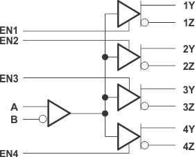 Figure 23. Example of Functional Block Diagram (SN65LVDS104)
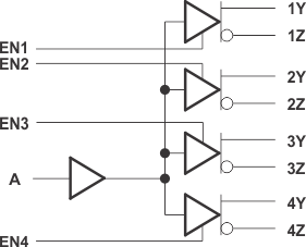 Figure 24. Example of Functional Block Diagram (SN65LVDS105)
9.3 Feature Description
9.3.1 Fail Safe
A common problem with differential signaling applications is how the system responds when no differential voltage is present on the signal pair. The LVDS receiver is like most differential line receivers, in that its output logic state can be indeterminate when the differential input voltage is between –100 mV and 100 mV and within its recommended input common-mode voltage range. However, TI LVDS receivers handles the open-input circuit situation differently.
Open-circuit means that there is little or no input current to the receiver from the data line itself. This could be when the driver is in a high-impedance state or the cable is disconnected. When this occurs, the LVDS receiver pulls each line of the signal pair to near VCC through 300-kΩ resistors as shown in Figure 25. The fail-safe feature uses an AND gate with input voltage thresholds at about 2.3 V to detect this condition and force the output to a high-level regardless of the differential input voltage.
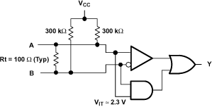 Figure 25. Open-Circuit Fail Safe of the LVDS Receiver
It is only under these conditions that the output of the receiver will be valid with less than a 100 mV differential input voltage magnitude. The presence of the termination resistor, Rt, does not affect the fail-safe function as long as it is connected as shown in Figure 25. Other termination circuits may allow a dc current to ground that could defeat the pullup currents from the receiver and the fail-safe feature.
9.4 Device Functional Modes
Table 2 lists the function tables for the SN65LVDS104 and 105 devices.
Table 2. Function Tables(1)
| SN65LVDS104 | SN65LVDS105 | ||||||
|---|---|---|---|---|---|---|---|
| INPUT | OUTPUT | INPUT | OUTPUT | ||||
| VID = VA - VB | xEN | xY | xZ | A | ENx | xY | xZ |
| X | X | Z | Z | L | H | L | H |
| X | L | Z | Z | H | H | H | L |
| VID ≥ 100 mV | H | H | L | Open | H | L | H |
| –100 mV < VID < 100 mV | H | ? | ? | X | L | Z | Z |
| VID ≤ –100 mV | H | L | H | X | X | Z | Z |
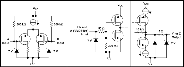 Figure 26. Equivalent Input and Output Schematic Diagrams
9.4.1 Input Level Translation
An LVDS receiver can be used to receive various other types of logic signals. Figure 27 through Figure 36 show the termination circuits for SSTL, HSTL, GTL, BTL, LVPECL, PECL, CMOS, and TTL.
 Figure 27. Sub-Series Terminated (SSTL) or High-Speed Transceiver Logic (HSTL)
 Figure 28. Center Tap Termination
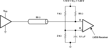 Figure 29. Gunning Transceiver Logic (GTL)
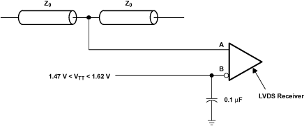 Figure 30. Backplane Transceiver
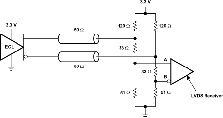 Figure 31. Low-Voltage Positive Emitter-Coupled Logic (LVPECL)
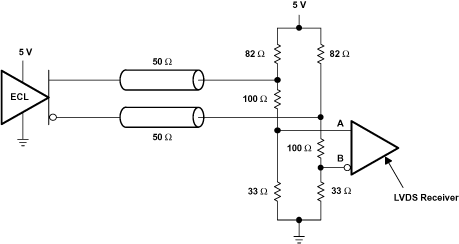 Figure 32. Positive Emitter-Coupled Logic (PECL)
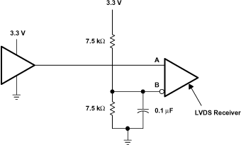 Figure 33. 3.3-V CMOS
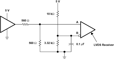 Figure 34. 5-V CMOS
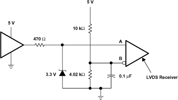 Figure 35. 5-V TTL
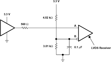 Figure 36. LVTTL