SLLS396G SEPTEMBER 1999 – December 2015 SN65LVDS104 , SN65LVDS105
PRODUCTION DATA.
- 1 Features
- 2 Applications
- 3 Description
- 4 Revision History
- 5 Selection Guide to LVDS Repeaters
- 6 Pin Configuration and Functions
-
7 Specifications
- 7.1 Absolute Maximum Ratings
- 7.2 ESD Ratings—JEDEC
- 7.3 ESD Ratings—MIL-STD
- 7.4 Recommended Operating Conditions
- 7.5 Thermal Information
- 7.6 SN65LVDS104 Electrical Characteristics
- 7.7 SN65LVDS105 Electrical Characteristics
- 7.8 SN65LVDS104 Switching Characteristics
- 7.9 SN65LVDS105 Switching Characteristics
- 7.10 Dissipation Ratings
- 7.11 Typical Characteristics
- 8 Parameter Measurement Information
- 9 Detailed Description
-
10Application and Implementation
- 10.1 Application Information
- 10.2
Typical Application
- 10.2.1 Point-to-Point Communications
- 10.2.2 Design Requirements
- 10.2.3
Detailed Design Procedure
- 10.2.3.1 Bypass Capacitance
- 10.2.3.2 Driver Supply Voltage
- 10.2.3.3 Driver Input Voltage
- 10.2.3.4 Driver Output Voltage
- 10.2.3.5 Interconnecting Media
- 10.2.3.6 PCB Transmission Lines
- 10.2.3.7 Termination Resistor
- 10.2.3.8 Receiver Supply Voltage
- 10.2.3.9 Receiver Input Common-Mode Range
- 10.2.3.10 Receiver Input Signal
- 10.2.3.11 Receiver Output Signal
- 10.2.4 Application Curve
- 10.3 Multidrop Communications
- 11Power Supply Recommendations
- 12Layout
- 13Device and Documentation Support
- 14Mechanical, Packaging, and Orderable Information
パッケージ・オプション
デバイスごとのパッケージ図は、PDF版データシートをご参照ください。
メカニカル・データ(パッケージ|ピン)
- PW|16
- D|16
サーマルパッド・メカニカル・データ
発注情報
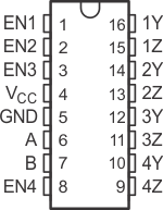
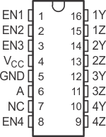
6 Pin Configuration and Functions
SN65LVDS104 D or PW Package
16-Pin SOIC or TSSOP
Top View

SN65LVDS105 D or PW Package
16-Pin SOIC or TSSOP
Top View

Pin Functions
| PIN | I/O | DESCRIPTION | ||
|---|---|---|---|---|
| NAME | SN65LVDS104 | SN65LVDS105 | ||
| A | 6 | 6 | I | LVDS input, positive (LVDS104) or LVTTL input, (LVDS105) |
| B | 7 | — | I | LVDS input, negative |
| EN1 | 1 | 1 | I | Enable, channel 1 |
| EN2 | 2 | 2 | I | Enable, channel 2 |
| EN3 | 3 | 3 | I | Enable, channel 3 |
| EN4 | 8 | 8 | I | Enable, channel 4 |
| GND | 5 | 5 | — | Ground |
| NC | — | 7 | — | No connect |
| VCC | 4 | 4 | — | Supply voltage |
| 1Y | 16 | 16 | O | LVDS output, positive, channel 1 |
| 1Z | 15 | 15 | O | LVDS output, negative, channel 1 |
| 2Y | 14 | 14 | O | LVDS output, positive, channel 2 |
| 2Z | 13 | 13 | O | LVDS output, negative, channel 2 |
| 3Y | 12 | 12 | O | LVDS output, positive, channel 3 |
| 3Z | 11 | 11 | O | LVDS output, negative, channel 3 |
| 4Y | 10 | 10 | O | LVDS output, positive, channel 4 |
| 4Z | 9 | 9 | O | LVDS output, negative, channel 4 |