JAJSKL8E june 2006 – october 2020 SN65LVDS302
PRODUCTION DATA
- 1
- 1 特長
- 2 アプリケーション
- 3 概要
- 4 Revision History
- 5 Pin Configuration and Functions
-
6 Specifications
- 6.1 Absolute Maximum Ratings
- 6.2 ESD Ratings
- 6.3 Recommended Operating Conditions
- 6.4 Thermal Information
- 6.5 Electrical Characteristics
- 6.6 Input Electrical Characteristics
- 6.7 Output Electrical Characteristics
- 6.8 Timing Requirements
- 6.9 Switching Characteristics
- 6.10 Device Power Dissipation
- Typical Characteristics
- 7 Parameter Measurement Information
- 8 Detailed Description
-
9 Application and Implementation
- 9.1
Application Information
- 9.1.1 Application Information
- 9.1.2 Preventing Increased Leakage Currents in Control Inputs
- 9.1.3 Calculation Example: HVGA Display
- 9.1.4 How to Determine Interconnect Skew and Jitter Budget
- 9.1.5 F/S Pin Setting and Connecting the SN65LVDS302 to an LCD Driver
- 9.1.6 How to Determine the LCD Driver Timing Margin
- 9.1.7 Typical Application Frequencies
- 9.2 Typical Applications
- 9.1
Application Information
- 10Power Supply Recommendations
- 11Layout
- 12Device and Documentation Support
- 13Mechanical, Packaging, and Orderable Information
9.1.6 How to Determine the LCD Driver Timing Margin
To determine the timing margin, it is necessary to specify the frequency of operation, identify the set-up and hold time of the LCD driver, and specify the output load of the SN65LVDS302 as a combination of the LCD driver input parasitics plus any capacitance caused by the connecting PCB trace. Furthermore, the setting of pin F/S and the SN65LVDS302 output skew impact the margin. The total remaining design margin calculates as following:
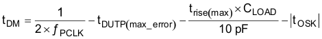
where
- tDM is the design margin
- fPCLK is the pixel clock frequency
- tDUTP(max_error) is the maximum duty cycle error
- trise(max) is the maximum rise or fall time; see tR/F under switching characteristics
- CL is the parasitic capacitance (sum of LCD driver input parasitics + connecting PCB trace)
- tskew is the clock to data output skew SN65LVDS302
Example:
At a pixel clock frequeny of 5.5 MHz (QVGA), and an assumed LCD driver load of 15 pF, the remaining timing margin is:
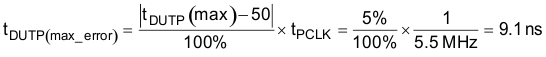
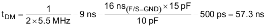
As long as the set-up and hold time of the LCD driver are each less than 57 ns, the timing budget is met sufficiently.