JAJSKL8E june 2006 – october 2020 SN65LVDS302
PRODUCTION DATA
- 1
- 1 特長
- 2 アプリケーション
- 3 概要
- 4 Revision History
- 5 Pin Configuration and Functions
-
6 Specifications
- 6.1 Absolute Maximum Ratings
- 6.2 ESD Ratings
- 6.3 Recommended Operating Conditions
- 6.4 Thermal Information
- 6.5 Electrical Characteristics
- 6.6 Input Electrical Characteristics
- 6.7 Output Electrical Characteristics
- 6.8 Timing Requirements
- 6.9 Switching Characteristics
- 6.10 Device Power Dissipation
- Typical Characteristics
- 7 Parameter Measurement Information
- 8 Detailed Description
-
9 Application and Implementation
- 9.1
Application Information
- 9.1.1 Application Information
- 9.1.2 Preventing Increased Leakage Currents in Control Inputs
- 9.1.3 Calculation Example: HVGA Display
- 9.1.4 How to Determine Interconnect Skew and Jitter Budget
- 9.1.5 F/S Pin Setting and Connecting the SN65LVDS302 to an LCD Driver
- 9.1.6 How to Determine the LCD Driver Timing Margin
- 9.1.7 Typical Application Frequencies
- 9.2 Typical Applications
- 9.1
Application Information
- 10Power Supply Recommendations
- 11Layout
- 12Device and Documentation Support
- 13Mechanical, Packaging, and Orderable Information
8.4.4 Status Detect and Operating Modes Flow
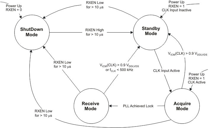
The SN65LVDS302 switches between the power saving and active modes in the following way:
 Figure 8-7 Operating Modes and State Machine Diagram
Table 8-2 Status Detect and Operating Modes Descriptions
| MODE | CHARACTERISTICS | CONDITIONS |
|---|---|---|
| Shutdown Mode | Least amount of power consumption (most circuitry turned off); All outputs held static: R[0:7] = G[0:7] = B[0:7] = VS = HS = high DE = PCLK = low; | RXEN is set low for longer than 10 μs(1)(2) |
| Standby Mode | Low power consumption (Standby monitor circuit active; PLL is shutdown to conserve power); All outputs held static: R[0:7] = G[0:7] = B[0:7] = VS = HS = high DE = PCLK = low; | RXEN is high for longer than 10 μs, and both CLK input common-mode VICM(CLK) above 0.9 × VDDLVDS, or CLK input floating(2) |
| Acquire Mode | PLL pursues lock; All outputs held static: R[0:7] = G[0:7] = B[0:7] = VS = HS = high DE = PCLK = low; | RXEN is high; CLK input monitor detected clock input common mode and woke up receiver out of Standby mode |
| Receive Mode | Data transfer (normal operation); receiver deserializes data and provides data on parallel output | RXEN is high and PLL is locked to incoming clock |
(1) In Shutdown Mode, all SN65LVDS302 internal switching circuits (for example: PLL, serializer, etc.) are turned off to minimize power consumption. The input stage of any input pin remains active.
(2) Leaving CMOS control inputs unconnected can cause random noise to toggle the input stage and potentially harm the device. All CMOS inputs must be tied to a valid logic level VIL or VIH during Shutdown or Standby Mode. Exceptions are the subLVDS inputs CLK and Dx, which can be left unconnected while not in use.
Table 8-3 Operating Mode Transitions
| MODE TRANSITION | USE CASE | TRANSITION SPECIFICS | |
|---|---|---|---|
| Shutdown → Standby | Drive RXEN high to enable receiver | 1. | RXEN high > 10 μs |
| 2. | Receiver enters standby mode | ||
| a. R[0:7] = G[0:7] = B[0:7] = VS = HS remain high and DE = PCLK low | |||
| b. Receiver activates clock input monitor | |||
| Standby → Acquire | Transmitter activity detected | 1. | CLK input monitor detects clock input activity |
| 2. | Outputs remain static | ||
| 3. | PLL circuit is enabled | ||
| Acquire → Receive | Link is ready to receive data | 1. | PLL is active and approaches lock |
| 2. | PLL achieves lock within twakeup | ||
| 3. | D1, D2, or D3 become active depending on LS0 and LS1 selection | ||
| 4. | First Data word was recovered | ||
| 5. | Parallel output bus turns on switching from static output pattern to output first valid data word | ||
| Receive → Standby | Transmitter requested to enter Standby mode by input common mode voltage VICM > 0.9 VDDLVDS as when transmitter output clock stops or enters high-impedance state. | 1. | Receiver disables outputs within tsleep |
| 2. | RX Input monitor detects VICM > 0.9 VDDLVDS within tsleep | ||
| 3. | R[0:7] = G[0:7] = B[0:7] = VS = HS transition to high and DE = PCLK to low on next falling PLL clock edge | ||
| 4. | PLL shuts down. Clock activity input monitor remains active | ||
| Receive and Standby → Shutdown | Turn off Receiver | 1. | RXEN pulled low for > tpwrdn |
| 2. | R[0:7] = G[0:7] = B[0:7] = VS = HS remain static high or transition to static high and DE = PCLK remain or transition to static low | ||
| 3. | Most IC circuitry is shut down for least power consumption | ||