JAJSF09B
February 2015 – April 2015
SN65LVDS93A-Q1
PRODUCTION DATA.
1
特長
2
アプリケーション
3
概要
概略回路図
4
改訂履歴
5
Pin Configuration and Functions
Pin Functions
6
Specifications
6.1
Absolute Maximum Ratings
6.2
ESD Ratings
6.3
Recommended Operating Conditions
6.4
Thermal Information
6.5
Electrical Characteristics
6.6
Timing Requirements
6.7
Switching Characteristics
6.8
Typical Characteristics
7
Parameter Measurement Information
8
Detailed Description
8.1
Overview
8.2
Functional Block Diagram
8.3
Feature Description
8.3.1
TTL Input Data
8.3.2
LVDS Output Data
8.4
Device Functional Modes
8.4.1
Input Clock Edge
8.4.2
Low Power Mode
9
Application and Implementation
9.1
Application Information
9.2
Typical Application
9.2.1
Design Requirements
9.2.2
Detailed Design Procedure
9.2.2.1
Power Up Sequence
9.2.2.2
Signal Connectivity
9.2.2.3
PCB Routing
9.2.3
Application Curve
10
Power Supply Recommendations
11
Layout
11.1
Layout Guidelines
11.1.1
Board Stackup
11.1.2
Power and Ground Planes
11.1.3
Traces, Vias, and Other PCB Components
11.2
Layout Example
12
デバイスおよびドキュメントのサポート
12.1
商標
12.2
静電気放電に関する注意事項
12.3
ドキュメントの更新通知を受け取る方法
12.4
コミュニティ・リソース
12.5
Glossary
13
メカニカル、パッケージ、および注文情報
パッケージ・オプション
メカニカル・データ(パッケージ|ピン)
DGG|56
MPDS570
サーマルパッド・メカニカル・データ
発注情報
jajsf09b_oa
jajsf09b_pm
9.2
Typical Application
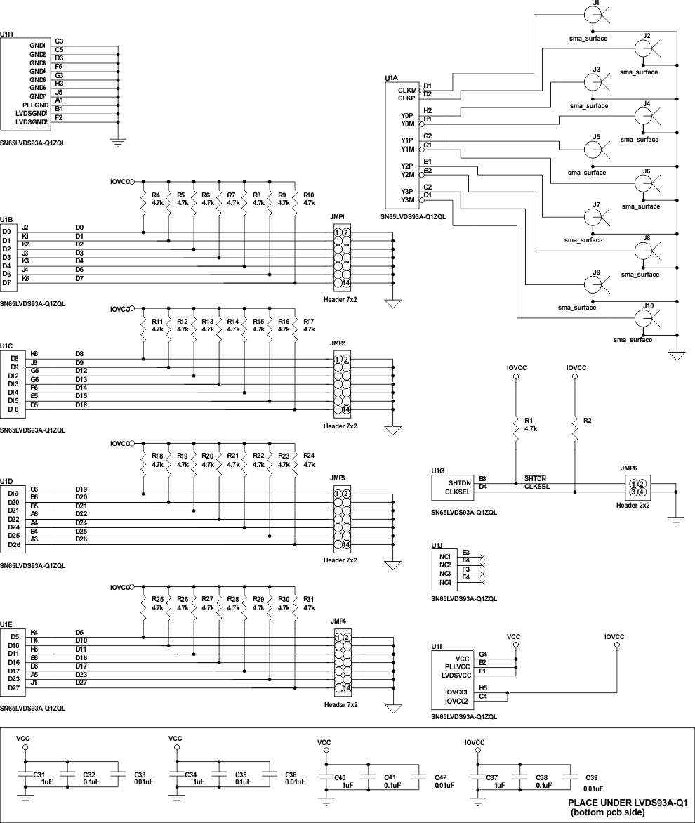
Figure 14.
Schematic Example (SN65LVDS93A-Q1 Evaluation Board)