JAJSF09B February 2015 – April 2015 SN65LVDS93A-Q1
PRODUCTION DATA.
11.1.2 Power and Ground Planes
A complete ground plane in high-speed design is essential. Additionally, a complete power plane is recommended as well. In a complex system, several regulated voltages can be present. The best solution is for every voltage to have its own layer and its own ground plane. But this would result in a huge number of layers just for ground and supply voltages. What are the alternatives? Split the ground planes and the power planes? In a mixed-signal design, e.g., using data converters, the manufacturer often recommends splitting the analog ground and the digital ground to avoid noise coupling between the digital part and the sensitive analog part. Take care when using split ground planes because:
- Split ground planes act as slot antennas and radiate.
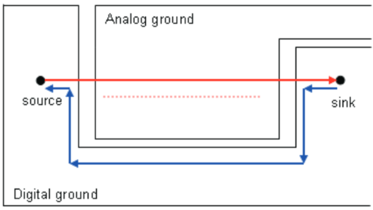
- A routed trace over a gap creates large loop areas, because the return current cannot flow beside the signal, and the signal can induce noise into the nonrelated reference plane (Figure 21).
- With a proper signal routing, crosstalk also can arise in the return current path due to discontinuities in the ground plane. Always take care of the return current (Figure 22).
For Figure 22, do not route a signal referenced to digital ground over analog ground and vice versa. The return current cannot take the direct way along the signal trace and so a loop area occurs. Furthermore, the signal induces noise, due to crosstalk (dotted red line) into the analog ground plane.
 Figure 21. Loop Area and Crosstalk Due to Poor Signal Routing and Ground Splitting
 Figure 22. Crosstalk Induced by the Return Current Path