SLLS516E August 2002 – July 2015 SN65LVDS100 , SN65LVDS101 , SN65LVDT100 , SN65LVDT101
UNLESS OTHERWISE NOTED, this document contains PRODUCTION DATA.
- 1 Features
- 2 Applications
- 3 Description
- 4 Revision History
- 5 Description (Continued)
- 6 Device Options
- 7 Pin Configuration and Functions
- 8 Specifications
- 9 Parameter Measurement Information
- 10Detailed Description
-
11Application and Implementation
- 11.1 Application Information
- 11.2
Typical Application
- 11.2.1 PECL to LVDS Translation
- 11.2.2 LVDS to 3.3-V PECL Translation
- 11.2.3 5-V PECL to 3.3-V PECL Translation
- 11.2.4 CML to LVDS or 3.3-V PECL Translation
- 11.2.5 Single-Ended 3.3-V PECL to LVDS Translation
- 11.2.6 Single-Ended CMOS to LVDS Translation
- 11.2.7 Single-Ended CMOS to 3.3-V PECL Translation
- 11.2.8 Receipt of AC-Coupled Signals
- 12Power Supply Recommendations
- 13Layout
- 14Device and Documentation Support
- 15Mechanical, Packaging, and Orderable Information
パッケージ・オプション
デバイスごとのパッケージ図は、PDF版データシートをご参照ください。
メカニカル・データ(パッケージ|ピン)
- D|8
- DGK|8
サーマルパッド・メカニカル・データ
発注情報
11 Application and Implementation
NOTE
Information in the following applications sections is not part of the TI component specification, and TI does not warrant its accuracy or completeness. TI’s customers are responsible for determining suitability of components for their purposes. Customers should validate and test their design implementation to confirm system functionality.
11.1 Application Information
The SN65LVDx10x are single-channel repeaters/translators. The functionality of these devices is simple, yet extremely flexible, leading to their use in designs ranging from wireless base stations to desktop computers. SN65LVDx10x devices are often used as buffers to regenerate or repeat the signal at their port. The devices in this family can accept any differential signal that meets the input port requirements specified herein. The input signal does not need to comply with any particular standard to be repeated: it just needs to fall within the common-mode input range of these devices, and have a differential input signal of at least 100 mV in magnitude. With such an input the designer can use a SN65LVDx100 device to repeat the digital input signal, and generate an output signal that carries the information at its input port, and complies with all the requirements of the LVDS standard. Similarly, an SN65LVDx101 device is a general-purpose differential receiver that repeats the input data at its output port, while complying with LVPECL output specifications.
Translating from one signaling standard to a different signaling standard is a common application issue. Two ICs that use different signaling standards may need to communicate with each other. An FPGA may output an LVDS signal and an ASIC may be designed to receive LVPECL inputs. Directly connecting the two devices would end up with communication errors. In such a case an SN65LVDS101 can be used to translate between the incompatible standards. The common application issue of converting from one standard to another are covered in Typical Application.
11.2 Typical Application
11.2.1 PECL to LVDS Translation
 Figure 41. PECL to LVDS Translation
11.2.1.1 Design Requirements
| DESIGN PARAMETER | EXAMPLE VALUE |
|---|---|
| PECL Source Supply Voltage (VCC) | 3.3 V |
| SN65LVDS100 Supply Voltage | 3.0 to 3.6 V |
| Driver Signaling Rate | DC to 2000 Mbps |
| Interconnect Characteristic Impedance | 100 Ω |
| Termination Resistance | 50 Ω to VCC – 2 V on each side of transmission line |
11.2.1.2 Detailed Design Requirements
Translating an LVPECL signal to LVDS is straightforward using the SN65LVDS100. The common-mode output of an LVPECL driver is approximately 2 V, while the differential output voltage would be approximately 600 to 800 mV. 2 V is right in the middle of the common-mode range of the SN65LVDS100, while the differential voltage is more than enough signal for the high-sensitivity receiver. As shown in Figure 41, 50-Ω pulldown resistors to VCC – 2 V are needed, and the rationale for these have been discussed earlier.
11.2.1.3 Application Curve
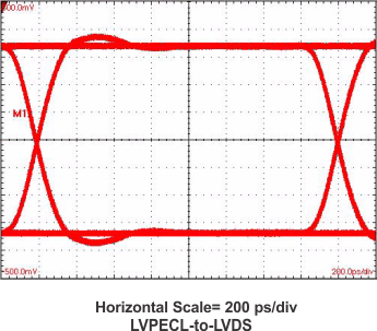 Figure 42. SN65LVDS100 Mbps, 223 – 1 PRBS
11.2.2 LVDS to 3.3-V PECL Translation
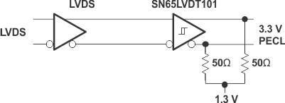 Figure 43. LVDS to 3.3-V PECL Translation
11.2.2.1 Design Requirements
| DESIGN PARAMETER | EXAMPLE VALUE |
|---|---|
| LVDS Source Supply Voltage (VCC) | 3.3 V |
| SN65LVDT101 Supply Voltage | 3.0 to 3.6 V |
| Driver Signaling Rate | DC to 2000 Mbps |
| Interconnect Characteristic Impedance | 100 Ω |
| Termination Resistance | Integrated in SN65LVDT101 |
11.2.2.2 Detailed Design Requirements
Translating an LVDS signal to LVPECL is conveniently done using the SN65LVDT101. The common-mode output of an LVDS driver is 1.2 V, while the differential output voltage would be approximately 350 mV. 1.2 V is well within the common-mode range of the SN65LVDT101, while the differential voltage is more than enough signal for the high-sensitivity receiver. The integrated variant of the LVPECL translators is used here as it includes precisely the load required for operation of an LVDS driver. This circuit is shown in Figure 43.
11.2.2.3 Application Curve
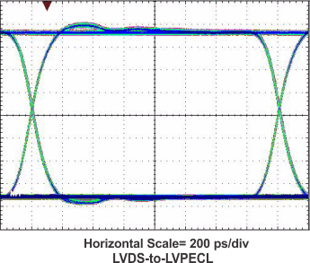 Figure 44. SN65LVDS101 Mbps, 223 – 1 PRBS
11.2.3 5-V PECL to 3.3-V PECL Translation
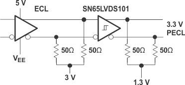 Figure 45. 5-V PECL to 3.3-V PECL Translation
11.2.3.1 Design Requirements
| DESIGN PARAMETER | EXAMPLE VALUE |
|---|---|
| PECL Source Supply Voltage (VCC) | 5.0 V |
| SN65LVDS101 Supply Voltage | 3.0 to 3.6 V |
| Driver Signaling Rate | DC to 2000 Mbps |
| Interconnect Characteristic Impedance | 100 Ω |
| Termination Resistance | 50 Ω to VCC – 2 V on each side of transmission line |
11.2.3.2 Detailed Design Requirements
At times a 5-V PECL will need to be converted to a 3.3-V PECL signal. When the 5-V signal is encoded (8b10b for example), ac-coupling can be used. Figure 45 shows how to translate a 5-V PECL signal to 3.3-V PECL when a dc connection is needed.
The 50-Ω pulldown resistors to VCC – 2 V are familiar by now. The SN65LVDS101 provides the 3.3-V based LVPECL signal.
A level of care must be exercised with this solution. The absolute voltage levels at the input pins to the SN65LVDS101 must be less than or equal to 4 V. With a 5-V PECL signal, the non-inverting output will generally be just below 4 V. If the 5-V PECL supply goes much above 5 V, the input voltage at the SN65LVDS101 may violate the specifications. Ensure that the worst-case high-output voltage from the 5-V PECL driver will be within the range of the SN65LVDS101.
11.2.3.3 Application Curve
Reference: Figure 44
11.2.4 CML to LVDS or 3.3-V PECL Translation
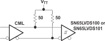 Figure 46. CML to LVDS or 3.3-V PECL Translation
11.2.4.1 Design Requirements
| DESIGN PARAMETER | EXAMPLE VALUE |
|---|---|
| CML Termination Supply Voltage (VTT) | 3.3 V |
| SN65LVDS10x Supply Voltage | 3.0 to 3.6 V |
| Driver Signaling Rate | DC to 2000 Mbps |
| Interconnect Characteristic Impedance | 100 Ω |
| Termination Resistance | 50 Ω to VTT on each side of transmission line |
11.2.4.2 Detailed Design Requirements
Current-mode logic (CML) signals are designed to drive a 100-Ω transmission line with a load termination being two 50-Ω pullup resistors to a power supply. This circuit is shown in Figure 46. Common CML drivers include 16-mA current sources that serve to develop the differential output signal. Using this 16-mA current source and assuming a 3.3-V CML driver is being used, the common-mode output of the driver in Figure 46 is 2.9 V and the differential output voltage is 800 mV. Both values are well within the operational envelope of the SN65LVDx10x family receivers.
To convert from 3.3-V CML signals to LVDS signals, the driver and receiver are connected in a straightforward fashion. The SN65LVDS100 is used in this circuit to convert to an LVDS output, while the SN65LVDS101 is used to convert to LVPECL.
Again, the reader will notice that the integrated termination devices in the SN65LVDx10x family are not mentioned for this conversion. The ‘LVDT devices incorporate a shunt 100-Ω termination which are not appropriate when a pullup termination is needed.
11.2.4.3 Application Curve
Reference: Figure 44
11.2.5 Single-Ended 3.3-V PECL to LVDS Translation
 Figure 47. Single-Ended 3.3-V PECL to LVDS Translation
11.2.5.1 Design Requirements
| DESIGN PARAMETER | EXAMPLE VALUE |
|---|---|
| ECL Supply Voltage | 3.3 V |
| SN65LVDS100 Supply Voltage | 3.0 to 3.6 V |
| Driver Signaling Rate | DC to 2000 Mbps |
| Interconnect Characteristic Impedance | 50 Ω |
| Termination Resistance | 50 Ω to GND |
| VBB Current to GND | 91 µA |
11.2.5.2 Detailed Design Requirements
The SN65LVDx10x family of devices provides the flexibility to translate single-ended input signals to differential outputs. The output can be either LVDS or LVPECL, depending on the choice of SN65LVDS10x that is used. Figure 47 demonstrates how to convert a single-ended LVPECL signal to an LVDS signal.
The common receiver used in this family will work with any pair of input signals that comply with its input requirements. In this example, let’s assume the single-sided LVPECL signal has a high-level voltage of VCC – 1 V = 2.3 V. Assume the low-level output voltage is VCC – 1.6 V = 1.7 V. The common-mode of these two levels is 2 V, which happens to be VCC – 1.3 V.
To use a single-ended signal with these receivers, we need to bias the unused input of the differential receiver. In this case we will bias the inverting input pin. With the high and low signal levels calculated above, we see the optimum bias point for the unused pin would be the common-mode or average signal level. The VBB pin provides this needed voltage. VBB has a nominal value of VCC – 1.35 V.
The 22-kΩ resistor in the circuit serves to limit the dc current being sourced by VBB. This resistor setting will limit the current to less than 100 μA, well within the recommended maximum value of 400 μA.
The drawback of a single-ended to differential-converted shown here is that the unused pin is being set to a fixed value that will be close to the signal common-mode voltage. Any deviation from VBB (in the actual signal common-mode) results in duty-cycle distortion at the differential output. Whether or not this is an issue is application dependent. If, for example, the input signal is a clock signal and clocking only happens on one edge, the distortion may be acceptable.
11.2.5.3 Application Curve
Reference: Figure 42
11.2.6 Single-Ended CMOS to LVDS Translation
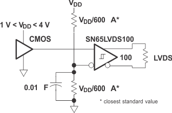 Figure 48. Single-Ended CMOS to LVDS Translation
11.2.6.1 Design Requirements
| DESIGN PARAMETER | EXAMPLE VALUE |
|---|---|
| CMOS Supply Voltage (VDD) | 1 V < VDD < 4 V |
| SN65LVDS100 Supply Voltage | 3.0 to 3.6 V |
| Driver Signaling Rate | DC to 500 Mbps |
| VBB Current to GND | 91 µA (VDD = 4 V) |
11.2.6.2 Detailed Design Requirements
The SN65LVDx10x family of devices can also translate a CMOS input signals to differential outputs. The output can be either LVDS or LVPECL, depending on the choice of SN65LVDS10x that is used. Figure 48 demonstrates how to convert a CMOS signal to an LVDS signal.
The CMOS signal in this case can be from any power rail up to 4 V (not a common rail, but the maximum allowable input at the receiver nonetheless). The unused or inverting signal in this case is biased to VDD/2 which will be equal to the common-mode of the CMOS input signal.
There is less concern with this circuit with regards to duty-cycle distortion, as we have assumed that the CMOS driver and the local voltage divider are referenced to the same rail. If different rails were used, the usual cautions on duty-cycle distortion would apply.
11.2.6.3 Application Curve
Reference: Figure 42
11.2.7 Single-Ended CMOS to 3.3-V PECL Translation
 Figure 49. Single-Ended CMOS to 3.3-V PECL Translation
11.2.7.1 Design Requirements
| DESIGN PARAMETER | EXAMPLE VALUE |
|---|---|
| CMOS Supply Voltage (VDD) | 1 V < VDD < 4 V |
| SN65LVDS101 Supply Voltage | 3.0 to 3.6 V |
| Driver Signaling Rate | DC to 500 Mbps |
| VBB Current to GND | 91 µA (VDD = 4 V) |
11.2.7.2 Detailed Design Requirements
Figure 49 demonstrates how to implement a CMOS to LVPECL translation. The elements in this circuit are now familiar, so the reader is referred to the previous discussions.
11.2.7.3 Application Curve
Reference: Figure 44
11.2.8 Receipt of AC-Coupled Signals
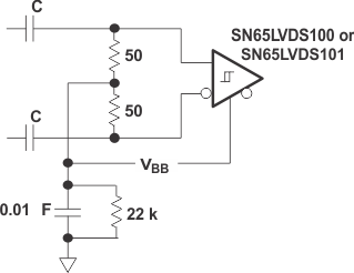 Figure 50. Receipt of AC-Coupled Signals
11.2.8.1 Design Requirements
| DESIGN PARAMETER | EXAMPLE VALUE |
|---|---|
| AC-coupling capacitor | 10 nF |
| SN65LVDS100 Supply Voltage | 3.0 to 3.6 V |
| Driver Signaling Rate | Up to 500 Mbps |
| VBB Current to GND | 91 µA (VDD = 4 V) |
| Low-Frequency Cutoff of RC Filter | 318 kHz |
11.2.8.2 Detailed Design Requirements
The general need to convert ac-coupled signals to either LVDS or LVPECL is shown in Figure 50. The transmission line is terminated with a center-tapped 100-Ω resistor network. The center tap is tied to the previously discussed VBB bias reference. The bias reference is current limited with the same 22-kΩ resistor to ground. The use of VBB is chosen for ease. This sets the common-mode at the receiver input approximately in the middle of the receiver input range (approximately 2 V).
The ac-coupling capacitors used on the input signal may be integrated into the source destination device, or may be discretely inserted on board. The capacitance value and the 50-Ω to ground terminations serve as a high-pass filter, blocking dc content. With a 10-nF capacitor the low-frequency zero is at 318 kHz. The reader needs to understand the frequency content of the incoming signal to determine whether this zero location is appropriate.
11.2.8.3 Application Curve
Reference: Figure 42