JAJSQM8E September 1998 – May 2024 SN74AHC08Q-Q1
PRODUCTION DATA
- 1
- 1特長
- 2概要
- 3Pin Configuration and Functions
- 4Specifications
- 5Parameter Measurement Information
- 6Detailed Description
- 7Device and Documentation Support
- 8Revision History
- 9Mechanical, Packaging, and Orderable Information
パッケージ・オプション
デバイスごとのパッケージ図は、PDF版データシートをご参照ください。
メカニカル・データ(パッケージ|ピン)
- D|14
- PW|14
- BQA|14
サーマルパッド・メカニカル・データ
- BQA|14
発注情報
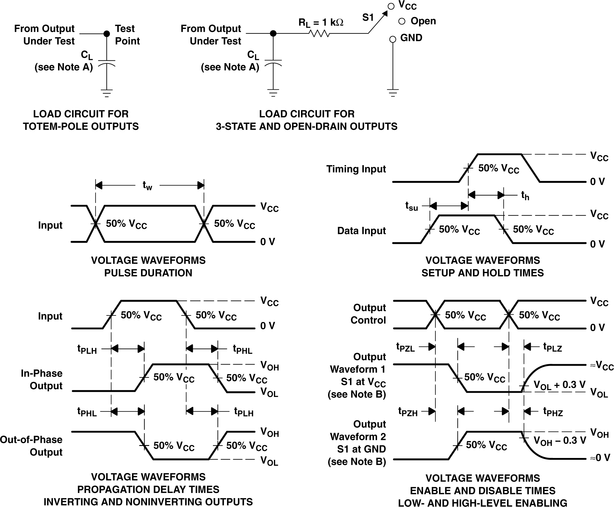
5 Parameter Measurement Information

A. CL includes probe and jig capacitance.
B. Waveform 1 is for an output with internal conditions such that the output is low, except when disabled by the output control. Waveform 2 is for an output with
internal conditions such that the output is high, except when disabled by the output control.
C. All input pulses are supplied by generators having the following characteristics: PRR ≤ 1 MHz, ZO = 50 Ω, tr ≤ 3 ns, tf ≤ 3
ns.
D. The outputs are measured one at a time, with one input transition per measurement.
Figure 5-1 Load Circuit and Voltage Waveforms| TEST | S1 |
|---|---|
| tPLH/tPHL | Open |
| tPLZ/tPZL | VCC |
| tPHZ/tPZH | GND |
| Open Drain | VCC |