SCLS334J March 1996 – October 2014 SN74AHCT16244
PRODUCTION DATA.
- 1 Features
- 2 Applications
- 3 Description
- 4 Simplified Schematic
- 5 Revision History
- 6 Pin Configuration and Functions
- 7 Specifications
- 8 Parameter Measurement Information
- 9 Detailed Description
- 10Application and Implementation
- 11Power Supply Recommendations
- 12Layout
- 13Device and Documentation Support
- 14Mechanical, Packaging, and Orderable Information
パッケージ・オプション
デバイスごとのパッケージ図は、PDF版データシートをご参照ください。
メカニカル・データ(パッケージ|ピン)
- DGG|48
- DL|48
- DGV|48
サーマルパッド・メカニカル・データ
発注情報
10 Application and Implementation
NOTE
Information in the following applications sections is not part of the TI component specification, and TI does not warrant its accuracy or completeness. TI’s customers are responsible for determining suitability of components for their purposes. Customers should validate and test their design implementation to confirm system functionality.
10.1 Application Information
The SN74HCT16244 is a low-drive CMOS device that can be used for a multitude of bus interface type applications where output ringing is a concern. The low drive and slow edge rates will minimize overshoot and undershoot on the outputs. The input switching levels have been lowered to accommodate TTL inputs of 0.8-V VIL and 2-V VIH. This feature makes it ideal for translating up from 3.3 V to 5 V. The figure below shows this type of translation
10.2 Typical Application
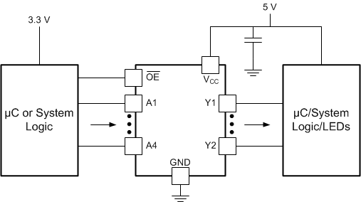 Figure 4. Typical Application Schematic
10.2.1 Design Requirements
This device uses CMOS technology and has balanced output drive. Care should be taken to avoid bus contention because it can drive currents that would exceed maximum limits. The high drive will also create fast edges into light loads, so routing and load conditions should be considered to prevent ringing.
10.2.2 Detailed Design Procedure
- Recommended Input Conditions:
- For rise time and fall time specifications, see Δt/ΔV in the Recommended Operating Conditions table.
- For specified high and low levels, see VIH and VIL in theRecommended Operating Conditions table.
- Inputs are overvoltage tolerant allowing them to go as high as 5.5 V at any valid VCC.
- Recommended Output Conditions:
- Load currents should not exceed 25 mA per output and 75 mA total for the part.
- Outputs should not be pulled above VCC.
10.2.3 Application Curves
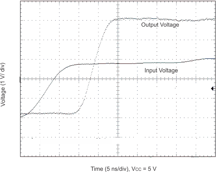 Figure 5. Up Translation