SCLS529E July 2003 – August 2024 SN74AHCT244-Q1
PRODMIX
- 1
- 1 Features
- 2 Applications
- 3 Description
- 4 Pin Configuration and Functions
- 5 Specifications
- 6 Parameter Measurement Information
- 7 Detailed Description
- 8 Application and Implementation
- 9 Device and Documentation Support
- 10Revision History
- 11Mechanical, Packaging, and Orderable Information
パッケージ・オプション
デバイスごとのパッケージ図は、PDF版データシートをご参照ください。
メカニカル・データ(パッケージ|ピン)
- PW|20
- DW|20
サーマルパッド・メカニカル・データ
発注情報
3 Description
This octal buffer/driver is designed specifically to improve both the performance and density of 3-state memory-address drivers, clock drivers, and bus-oriented receivers and transmitters.
Package Information
| PART NUMBER | PACKAGE(1) | PACKAGE SIZE(2) | BODY SIZE(3) |
|---|---|---|---|
| SN74AHCT244-Q1 | DW (SOIC, 20) | 12.80mm × 10.3mm | 12.8mm x 7.5mm |
| PW (TSSOP, 20) | 6.50mm × 6.4mm | 6.50mm x 4.40mm |
(1) For more information, see Section 11.
(2) The package size (length × width) is
a nominal value and includes pins, where applicable.
(3) The body size (length × width) is
a nominal value and does not include pins.
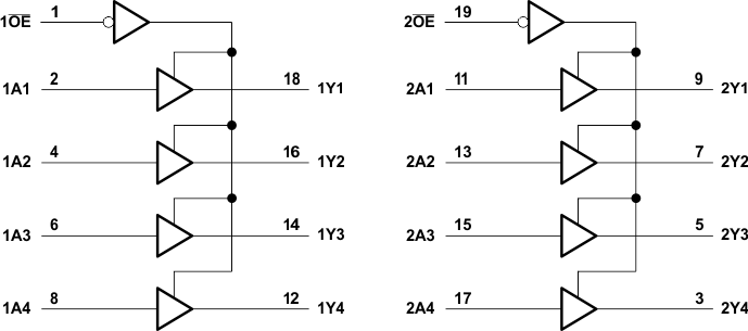
 Logic Diagram (Positive Logic)