JAJSQW1O October 1995 – August 2024 SN54AHCT373 , SN74AHCT373
PRODMIX
- 1
- 1 特長
- 2 概要
- 3 Pin Configuration and Functions
- 4 Specifications
- 5 Parameter Measurement Information
- 6 Detailed Description
- 7 Application and Implementation
- 8 Device and Documentation Support
- 9 Revision History
- 10Mechanical, Packaging, and Orderable Information
パッケージ・オプション
デバイスごとのパッケージ図は、PDF版データシートをご参照ください。
メカニカル・データ(パッケージ|ピン)
- DB|20
- NS|20
- N|20
- DW|20
- PW|20
サーマルパッド・メカニカル・データ
発注情報
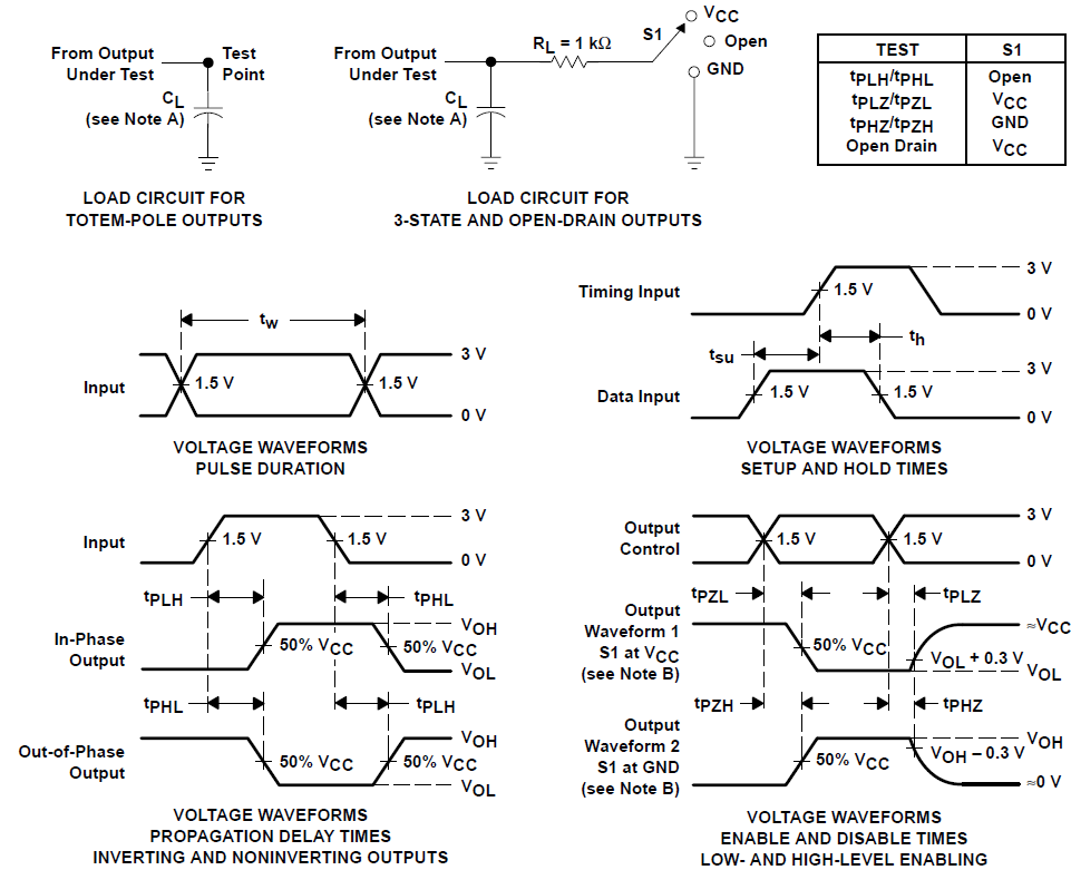
5 Parameter Measurement Information

NOTES: A. CL includes probe and jig capacitance.
B. Waveform 1 is for an output with internal conditions such that the output is low except when disabled by the output control. Waveform 2 is for an output with internal conditions such that the output is high except when disabled by the output control.
C. All input pulses are supplied by generators having the following characteristics: PRR ≤ 1 MHz, Z O = 50 Ω, tr ≤ 3 ns, tf ≤ 3 ns.
D. The outputs are measured one at a time with one input transition per measurement.
E. All parameters and waveforms are not applicable to all devices.
Figure 5-1 Load Circuit and Voltage Waveforms