JAJSI03K June 2004 – May 2020 SN74AUP1G32
PRODUCTION DATA
- 1 特長
- 2 アプリケーション
- 3 概要
- 4 Revision History
- 5 Pin Configuration and Functions
-
6 Specifications
- 6.1 Absolute Maximum Ratings
- 6.2 Handling Ratings
- 6.3 Recommended Operating Conditions
- 6.4 Thermal Information
- 6.5 Electrical Characteristics
- 6.6 Switching Characteristics, CL = 5 pF
- 6.7 Switching Characteristics, CL = 10 pF
- 6.8 Switching Characteristics, CL = 15 pF
- 6.9 Switching Characteristics, CL = 30 pF
- 6.10 Operating Characteristics
- 6.11 Typical Characteristics
- 7 Parameter Measurement Information
- 8 Detailed Description
- 9 Application and Implementation
- 10Power Supply Recommendations
- 11Layout
- 12Device and Documentation Support
- 13Mechanical, Packaging, and Orderable Information
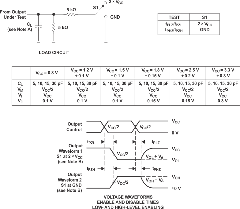
7.2 Enable and Disable Times

A. CL includes probe and jig capacitance.
B.
C. All input pulses are supplied by generators having the following characteristics: PRR ≤ 10 MHz, ZO = 50 Ω,
tr and tf = 3 ns.
tr and tf = 3 ns.
D. The outputs are measured one at a time, with one transition per measurement.
E. tPLZ and tPHZ are the same as tdis.
F. tPZL and tPZH are the same as ten.
G. All parameters and waveforms are not applicable to all devices.
Figure 7-2 Load Circuit and Voltage Waveforms