SCES852A December 2013 – April 2016 SN74AUP1T34-Q1
PRODUCTION DATA.
- 1 Features
- 2 Applications
- 3 Description
- 4 Revision History
- 5 Pin Configuration and Functions
- 6 Specifications
- 7 Parameter Measurement Information
- 8 Detailed Description
- 9 Application and Implementation
- 10Power Supply Recommendations
- 11Layout
- 12Device and Documentation Support
- 13Mechanical, Packaging, and Orderable Information
9 Application and Implementation
NOTE
Information in the following applications sections is not part of the TI component specification, and TI does not warrant its accuracy or completeness. TI’s customers are responsible for determining suitability of components for their purposes. Customers should validate and test their design implementation to confirm system functionality.
9.1 Application Information
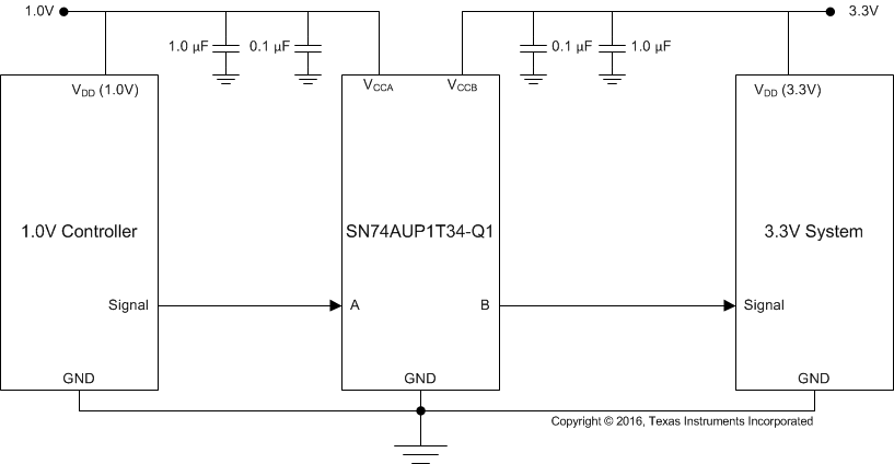
The SN74AUP1T34-Q1 can be used in level-translation applications for interfacing devices or systems operating at different interface voltages with one another.
9.2 Typical Application
 Figure 4. Typical Application Example
9.2.1 Design Requirements
Table 2 lists the design requirements of the SN74AUP1T34-Q1.
Table 2. Design Parameters
| DESIGN PARAMETER | EXAMPLE VALUE |
|---|---|
| Input Voltage Range | 0.9 V to 3.6 V |
| Output Voltage Range | 0.9 V to 3.6 V |
9.2.2 Detailed Design Procedure
To begin the design process, determine the following:
- Input voltage range
- Use the supply voltage of the device that is driving the SN74AUP1T34-Q1 device to determine the input voltage range. For a valid logic-high, the value must exceed the VIH of the input port. For a valid logic low the value must be less than the VIL of the input port.
- Output voltage range
- Use the supply voltage of the device that the SN74AUP1T34-Q1 device is driving to determine the output voltage range.
9.2.3 Application Curve
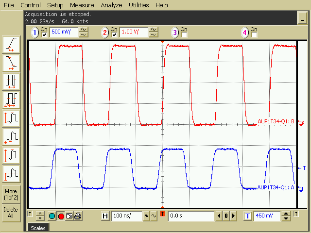
 Figure 5. 10 MHz Up Translation (0.9 V to 3.6 V)