SCES852A December 2013 – April 2016 SN74AUP1T34-Q1
PRODUCTION DATA.
- 1 Features
- 2 Applications
- 3 Description
- 4 Revision History
- 5 Pin Configuration and Functions
- 6 Specifications
- 7 Parameter Measurement Information
- 8 Detailed Description
- 9 Application and Implementation
- 10Power Supply Recommendations
- 11Layout
- 12Device and Documentation Support
- 13Mechanical, Packaging, and Orderable Information
8 Detailed Description
8.1 Overview
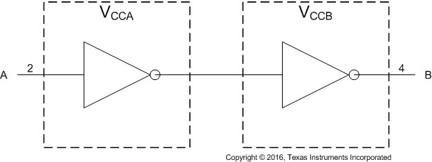
The SN74AUP1T34-Q1 is a unidirectional, single-bit, dual-supply, noninverting voltage-level translator. Pin A, which is referenced to VCCA, receives the signal that is to be level translated. Pin B, which is referenced to VCCB, transmits the level translated signal. Both supply pins VCCA and VCCB support a voltage range from 0.9 V to
3.6 V.
8.2 Functional Block Diagram

8.3 Feature Description
8.3.1 Fully Configurable Dual-Rail Design
Both VCCA and VCCB can be supplied at any voltage from 0.9 V to 3.6 V, making the device suitable for translating between any of the voltage nodes (1 V, 1.2 V, 1.8 V, 2.5 V, and 3.3 V).
8.3.2 Partial-Power-Down Mode Operation
Ioff circuitry disables the outputs, preventing damaging current backflow through the SN74AUP1T34-Q1 when it is powered down. This can occur in applications where subsections of a system are powered down (partial-power-down) to reduce power consumption.
8.3.3 VCC Isolation
The VCC isolation feature ensures that if either VCCA or VCCB are at GND (or < 0.4 V), both ports A and B are set to a high-impedance state, preventing false logic levels from being presented to either bus.
8.3.4 Input Hysteresis
Input hysteresis allows the input to support slew rates as slow as 200 ns/V, improving switching noise immunity.
8.4 Device Functional Modes
Table 1 lists the functional modes of the SN74AUP1T34-Q1.
Table 1. Function Table
| INPUT | OUTPUT |
|---|---|
| A PORT | B PORT |
| L | L |
| H | H |