JAJSUL6 May 2024 SN74AVC1T45-Q1
PRODUCTION DATA
- 1
- 1 特長
- 2 アプリケーション
- 3 概要
- 4 Pin Configuration and Functions
-
5 Specifications
- 5.1 Absolute Maximum Ratings
- 5.2 ESD Ratings
- 5.3 Recommended Operating Conditions
- 5.4 Thermal Information
- 5.5 Electrical Characteristics
- 5.6 Switching Characteristics, VCCA = 1.2 ± 0.12V
- 5.7 Switching Characteristics, VCCA = 1.5 ± 0.1V
- 5.8 Switching Characteristics, VCCA = 1.8 ± 0.15V
- 5.9 Switching Characteristics, VCCA = 2.5 ± 0.2V
- 5.10 Switching Characteristics, VCCA = 3.3 ± 0.3V
- 5.11 Operating Characteristics
- 5.12 Typical Characteristics
- 6 Parameter Measurement Information
- 7 Detailed Description
- 8 Application and Implementation
- 9 Device and Documentation Support
- 10Revision History
- 11Mechanical, Packaging, and Orderable Information
パッケージ・オプション
デバイスごとのパッケージ図は、PDF版データシートをご参照ください。
メカニカル・データ(パッケージ|ピン)
- DCK|6
サーマルパッド・メカニカル・データ
発注情報
8.2.2 Bidirectional Logic Level-Shifting Application
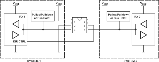
Figure 8-3 shows the SN74AVC1T45-Q1 being used in a bidirectional logic level-shifting application. Because the SN74AVC1T45-Q1 does not have an output-enable (OE) pin, the system designer should take precautions to avoid bus contention between SYSTEM-1 and SYSTEM-2 when changing directions.
 Figure 8-3 Bidirectional Logic Level-Shifting Application
The following table provides data transmission from SYSTEM-1 to SYSTEM-2 and then from SYSTEM-2 to SYSTEM-1.
| STATE | DIR CTRL | I/O-1 | I/O-2 | DESCRIPTION |
|---|---|---|---|---|
| 1 | H | Out | In | SYSTEM-1 data to SYSTEM-2 |
| 2 | H | Hi-Z | Hi-Z | SYSTEM-2 is getting ready to send data to SYSTEM-1. I/O-1 and I/O-2 are disabled. The bus-line state depends on pullup or pulldown.(1) |
| 3 | L | Hi-Z | Hi-Z | DIR bit is flipped. I/O-1 and I/O-2 still are disabled. The bus-line state depends on pullup or pulldown.(1) |
| 4 | L | In | Out | SYSTEM-2 data to SYSTEM-1 |