JAJSKB8E June 2008 – September 2024 SN74AVC2T245
PRODUCTION DATA
- 1
- 1 特長
- 2 アプリケーション
- 3 概要
- 4 Pin Configuration and Functions
-
5 Specifications
- 5.1 Absolute Maximum Ratings
- 5.2 ESD Ratings
- 5.3 Recommended Operating Conditions
- 5.4 Thermal Information
- 5.5 Electrical Characteristics
- 5.6 Switching Characteristics: VCCA = 1.2 V
- 5.7 Switching Characteristics: VCCA = 1.5 V ± 0.1 V
- 5.8 Switching Characteristics: VCCA = 1.8 V ± 0.15 V
- 5.9 Switching Characteristics: VCCA = 2.5 V ± 0.2 V
- 5.10 Switching Characteristics: VCCA = 3.3 V ± 0.3 V
- 5.11 Operating Characteristics
- 5.12 Typical Characteristics
- 6 Parameter Measurement Information
- 7 Detailed Description
- 8 Application and Implementation
- 9 Power Supply Recommendations
- 10Layout
- 11Device and Documentation Support
- 12Revision History
- 13Mechanical, Packaging, and Orderable Information
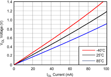
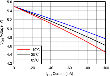
5.12 Typical Characteristics

