JAJSJB8B June 2011 – July 2020 SN74AVC4T234
PRODUCTION DATA
- 1 特長
- 2 アプリケーション
- 3 概要
- 4 Revision History
- 5 Pin Configuration and Functions
-
6 Specifications
- 6.1 Absolute Maximum Ratings
- 6.2 ESD Ratings
- 6.3 Recommended Operating Conditions
- 6.4 Thermal Information
- 6.5 Electrical Characteristics
- 6.6 Switching Characteristics, VCCB = 1.1 V
- 6.7 Switching Characteristics, VCCB = 1.4 V
- 6.8 Switching Characteristics, VCCB = 1.65 V
- 6.9 Switching Characteristics, VCCB = 2.3 V
- 6.10 Switching Characteristics, VCCB = 3 V
- 6.11 Operating Characteristics
- 7 Parameter Measurement Information
- 8 Detailed Description
- 9 Application and Implementation
- 10Power Supply Recommendations
- 11Layout
- 12Device and Documentation Support
- 13Mechanical, Packaging, and Orderable Information
5 Pin Configuration and Functions
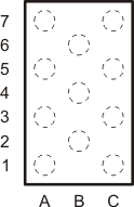
 Figure 5-1 ZSU/ZWA
Package
11-Pin uCSP
Transparent Top View
Figure 5-1 ZSU/ZWA
Package
11-Pin uCSP
Transparent Top ViewPin Functions
| PIN | NO. | TYPE | DESCRIPTION |
|---|---|---|---|
| NAME | ZSU, ZWA | ||
| B1 | C7 | I | Channel 1 Data input port |
| B2 | C5 | I | Channel 2 Data input port |
| B3 | C3 | I | Channel 3 Data input port |
| B4 | C1 | I | Channel 4 Data input port |
| A1 | A7 | O | Channel 1 Data output port |
| A2 | A5 | O | Channel 2 Data output port |
| A3 | A3 | O | Channel 3 Data output port |
| A4 | A1 | O | Channel 4 Data output port |
| VCCA | B6 | — | A-side output port power supply voltage (0.9 V to 3.6 V) |
| VCCB | B4 | — | B-side input port power supply voltage (0.9 V to 3.6 V) |
| GND | B2 | — | Ground |