SCES908A February 2020 – April 2020 SN74AXC2T245-Q1
PRODUCTION DATA.
- 1 Features
- 2 Applications
- 3 Description
- 4 Revision History
- 5 Pin Configuration and Functions
-
6 Specifications
- 6.1 Absolute Maximum Ratings
- 6.2 ESD Ratings
- 6.3 Recommended Operating Conditions
- 6.4 Thermal Information
- 6.5 Electrical Characteristics
- 6.6 Switching Characteristics, VCCA = 0.7 ± 0.05 V
- 6.7 Switching Characteristics, VCCA = 0.8 ± 0.04 V
- 6.8 Switching Characteristics, VCCA = 0.9 ± 0.045 V
- 6.9 Switching Characteristics, VCCA = 1.2 ± 0.1 V
- 6.10 Switching Characteristics, VCCA = 1.5 ± 0.1 V
- 6.11 Switching Characteristics, VCCA = 1.8 ± 0.15 V
- 6.12 Switching Characteristics, VCCA = 2.5 ± 0.2 V
- 6.13 Switching Characteristics, VCCA = 3.3 ± 0.3 V
- 6.14 Operating Characteristics: TA = 25°C
- 7 Parameter Measurement Information
-
8 Detailed Description
- 8.1 Overview
- 8.2 Functional Block Diagram
- 8.3
Feature Description
- 8.3.1 Standard CMOS Inputs
- 8.3.2 Balanced High-Drive CMOS Push-Pull Outputs
- 8.3.3 Partial Power Down (Ioff)
- 8.3.4 VCC Isolation
- 8.3.5 Over-voltage Tolerant Inputs
- 8.3.6 Glitch-free Power Supply Sequencing
- 8.3.7 Negative Clamping Diodes
- 8.3.8 Fully Configurable Dual-Rail Design
- 8.3.9 Supports High-Speed Translation
- 8.4 Device Functional Modes
- 9 Application and Implementation
- 10Power Supply Recommendations
- 11Layout
- 12Device and Documentation Support
- 13Mechanical, Packaging, and Orderable Information
3 Description
The SN74AXC2T245-Q1 is a two-bit noninverting bus transceiver that uses two individually configurable power-supply rails. The device is operational with both VCCA and VCCB supplies as low as 0.65 V. The A port is designed to track VCCA, which accepts any supply voltage from 0.65 V to 3.6 V. The B port is designed to track VCCB, which also accepts any supply voltage from 0.65 V to 3.6 V. Additionally the SN74AXC2T245-Q1 is compatible with a single-supply system.
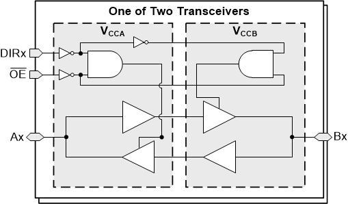
The SN74AXC2T245-Q1 device is designed for asynchronous communication between data buses. The device transmits data from the A bus to the B bus or from the B bus to the A bus, depending on the logic level of the direction-control inputs (DIRx). The SN74AXC2T245-Q1 device is designed so the control pin (DIR) is referenced to VCCA.
This device is fully specified for partial-power-down applications using the Ioff current. The Ioff protection circuitry ensures that no excessive current is drawn from or to an input, output, or combined I/O that is biased to a specific voltage while the device is powered down.
The VCC isolation feature ensures that if either VCCA or VCCB is less than 100 mV, both I/O ports enter a high-impedance state by disabling their outputs.
Glitch-free power supply sequencing allows either supply rail to be powered on or off in any order while providing robust power sequencing performance.
Device Information(1)
| PART NUMBER | PACKAGE | BODY SIZE (NOM) |
|---|---|---|
| CAXC2T245QRSWRQ1 | UQFN (10) | 1.80 mm x 1.40 mm |
- For all available packages, see the orderable addendum at the end of the data sheet.
Functional Block Diagram
