SCES908A February 2020 – April 2020 SN74AXC2T245-Q1
PRODUCTION DATA.
- 1 Features
- 2 Applications
- 3 Description
- 4 Revision History
- 5 Pin Configuration and Functions
-
6 Specifications
- 6.1 Absolute Maximum Ratings
- 6.2 ESD Ratings
- 6.3 Recommended Operating Conditions
- 6.4 Thermal Information
- 6.5 Electrical Characteristics
- 6.6 Switching Characteristics, VCCA = 0.7 ± 0.05 V
- 6.7 Switching Characteristics, VCCA = 0.8 ± 0.04 V
- 6.8 Switching Characteristics, VCCA = 0.9 ± 0.045 V
- 6.9 Switching Characteristics, VCCA = 1.2 ± 0.1 V
- 6.10 Switching Characteristics, VCCA = 1.5 ± 0.1 V
- 6.11 Switching Characteristics, VCCA = 1.8 ± 0.15 V
- 6.12 Switching Characteristics, VCCA = 2.5 ± 0.2 V
- 6.13 Switching Characteristics, VCCA = 3.3 ± 0.3 V
- 6.14 Operating Characteristics: TA = 25°C
- 7 Parameter Measurement Information
-
8 Detailed Description
- 8.1 Overview
- 8.2 Functional Block Diagram
- 8.3
Feature Description
- 8.3.1 Standard CMOS Inputs
- 8.3.2 Balanced High-Drive CMOS Push-Pull Outputs
- 8.3.3 Partial Power Down (Ioff)
- 8.3.4 VCC Isolation
- 8.3.5 Over-voltage Tolerant Inputs
- 8.3.6 Glitch-free Power Supply Sequencing
- 8.3.7 Negative Clamping Diodes
- 8.3.8 Fully Configurable Dual-Rail Design
- 8.3.9 Supports High-Speed Translation
- 8.4 Device Functional Modes
- 9 Application and Implementation
- 10Power Supply Recommendations
- 11Layout
- 12Device and Documentation Support
- 13Mechanical, Packaging, and Orderable Information
8.3.7 Negative Clamping Diodes
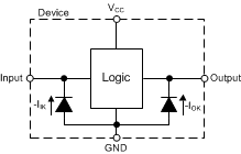
The inputs and outputs to this device have negative clamping diodes as depicted in Figure 5.
CAUTION
Voltages beyond the values specified in the Absolute Maximum Ratings table can cause damage to the device. The input negative-voltage and output voltage ratings may be exceeded if the input and output clamp-current ratings are observed.
 Figure 5. Electrical Placement of Clamping Diodes for Each Input and Output