JAJSH74B December 2018 – April 2024 SN74AXC4T245
PRODUCTION DATA
- 1
- 1 特長
- 2 アプリケーション
- 3 概要
- 4 Pin Configuration and Functions
-
5 Specifications
- 5.1 Absolute Maximum Ratings
- 5.2 ESD Ratings
- 5.3 Recommended Operating Conditions
- 5.4 Thermal Information
- 5.5 Electrical Characteristics
- 5.6 Switching Characteristics, VCCA = 0.7V
- 5.7 Switching Characteristics, VCCA = 0.8V
- 5.8 Switching Characteristics, VCCA = 0.9V
- 5.9 Switching Characteristics, VCCA = 1.2V
- 5.10 Switching Characteristics, VCCA = 1.5V
- 5.11 Switching Characteristics, VCCA = 1.8V
- 5.12 Switching Characteristics, VCCA = 2.5V
- 5.13 Switching Characteristics, VCCA = 3.3V
- 5.14 Operating Characteristics: TA = 25°C
- 6 Parameter Measurement Information
-
7 Detailed Description
- 7.1 Overview
- 7.2 Functional Block Diagram
- 7.3
Feature Description
- 7.3.1 Standard CMOS Inputs
- 7.3.2 Balanced High-Drive CMOS Push-Pull Outputs
- 7.3.3 Partial Power Down (Ioff)
- 7.3.4 VCC Isolation
- 7.3.5 Over-voltage Tolerant Inputs
- 7.3.6 Glitch-free Power Supply Sequencing
- 7.3.7 Negative Clamping Diodes
- 7.3.8 Fully Configurable Dual-Rail Design
- 7.3.9 I/Os with Integrated Static Pull-Down Resistors
- 7.3.10 Supports High-Speed Translation
- 7.4 Device Functional Modes
- 8 Application and Implementation
- 9 Device and Documentation Support
- 10Revision History
- 11Mechanical, Packaging, and Orderable Information
パッケージ・オプション
デバイスごとのパッケージ図は、PDF版データシートをご参照ください。
メカニカル・データ(パッケージ|ピン)
- PW|16
- BQB|16
- RSV|16
サーマルパッド・メカニカル・データ
- BQB|16
発注情報
4 Pin Configuration and Functions
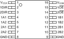
 Figure 4-1 PW Package
16-Pin TSSOP
(Top View)
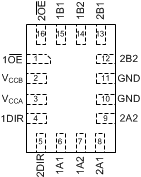
 Figure 4-3 RSV Package
16-Pin UQFN
(Transparent Top View)
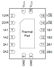
 Figure 4-2 BQB Package
16-Pin WQFN
(Transparent Top View)
Figure 4-2 BQB Package
16-Pin WQFN
(Transparent Top View)Table 4-1 Pin Functions
| PIN | NO. | TYPE(1) | DESCRIPTION | ||
|---|---|---|---|---|---|
| NAME | PW | RSV | BQB | ||
| 1A1 | 4 | 6 | 4 | I/O | Input/output 1A1. Referenced to VCCA. |
| 1A2 | 5 | 7 | 5 | I/O | Input/output 1A2. Referenced to VCCA. |
| 1B1 | 13 | 15 | 13 | I/O | Input/output 1B1. Referenced to VCCB. |
| 1B2 | 12 | 14 | 12 | I/O | Input/output 1B2. Referenced to VCCB. |
| 1DIR | 2 | 4 | 2 | I | Direction-control input for ‘1’ ports. |
| 1 OE | 15 | 1 | 15 | I | Tri-state output-mode enable. Pull OE high to place ‘1’ outputs in tri-state mode. Referenced to VCCA. |
| 2A1 | 6 | 8 | 6 | I/O | Input/output 2A1. Referenced to VCCA. |
| 2A2 | 7 | 9 | 7 | I/O | Input/output 2A2. Referenced to VCCA. |
| 2B1 | 11 | 13 | 11 | I/O | Input/output 2B1. Referenced to VCCB. |
| 2B2 | 10 | 12 | 10 | I/O | Input/output 2B2. Referenced to VCCB. |
| 2DIR | 3 | 5 | 3 | I | Direction-control input for ‘2’ ports. |
| 2 OE | 14 | 16 | 14 | I | Tri-state output-mode enable. Pull OE high to place ‘2’ outputs in tri-state mode. Referenced to VCCA. |
| GND | 8, 9 | 10, 11 | 8, 9 | — | Ground. |
| VCCA | 1 | 3 | 1 | — | A-port power supply voltage. 0.65V ≤ VCCA ≤ 3.6V. |
| VCCB | 16 | 2 | 16 | — | B-port power supply voltage. 0.65V ≤ VCCB ≤ 3.6V. |
(1) I = input, O = output