JAJSH48 March 2019 SN74AXCH4T245
PRODUCTION DATA.
- 1 特長
- 2 アプリケーション
- 3 概要
- 4 改訂履歴
- 5 概要(続き)
- 6 Pin Configuration and Functions
-
7 Specifications
- 7.1 Absolute Maximum Ratings
- 7.2 ESD Ratings
- 7.3 Recommended Operating Conditions
- 7.4 Thermal Information
- 7.5 Electrical Characteristics
- 7.6 Switching Characteristics, VCCA = 0.7 ± 0.05 V
- 7.7 Switching Characteristics, VCCA = 0.8 ± 0.04 V
- 7.8 Switching Characteristics, VCCA = 0.9 ± 0.045 V
- 7.9 Switching Characteristics, VCCA = 1.2 ± 0.1 V
- 7.10 Switching Characteristics, VCCA = 1.5 ± 0.1 V
- 7.11 Switching Characteristics, VCCA = 1.8 ± 0.15 V
- 7.12 Switching Characteristics, VCCA = 2.5 ± 0.2 V
- 7.13 Switching Characteristics, VCCA = 3.3 ± 0.3 V
- 7.14 Operating Characteristics: TA = 25°C
- 7.15 Typical Characteristics
- 8 Parameter Measurement Information
-
9 Detailed Description
- 9.1 Overview
- 9.2 Functional Block Diagram
- 9.3
Feature Description
- 9.3.1 Standard CMOS Inputs
- 9.3.2 Balanced High-Drive CMOS Push-Pull Outputs
- 9.3.3 Partial Power Down (Ioff)
- 9.3.4 VCC Isolation
- 9.3.5 Over-voltage Tolerant Inputs
- 9.3.6 Glitch-free Power Supply Sequencing
- 9.3.7 Negative Clamping Diodes
- 9.3.8 Fully Configurable Dual-Rail Design
- 9.3.9 Supports High-Speed Translation
- 9.3.10 Bus-Hold Data Inputs
- 9.4 Device Functional Modes
- 10Application and Implementation
- 11Power Supply Recommendations
- 12Layout
- 13デバイスおよびドキュメントのサポート
- 14メカニカル、パッケージ、および注文情報
パッケージ・オプション
メカニカル・データ(パッケージ|ピン)
サーマルパッド・メカニカル・データ
発注情報
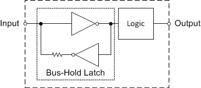
9.3.10 Bus-Hold Data Inputs
Each data input on this device includes a weak latch that maintains a valid logic level on the input. The state of these latches is unknown at startup and remains unknown until the input has been forced to a valid high or low state. After data has been sent through a channel, the latch then maintains the previous state on the input if the line is left floating. It is not recommended to use pull-up or pull-down resistors together with a bus-hold input, as it may cause undefined inputs to occur which leads to excessive current consumption.
Bus-hold data inputs prevent floating inputs on this device. The Implications of Slow or Floating CMOS Inputs application report explains the problems associated with leaving CMOS inputs floating.
These latches remain active at all times, independent of all control signals such as direction control or output enable.
The Bus-Hold Circuit application report has additional details regarding bus-hold inputs.
 Figure 10. Simplified Schematic For Device With Bus-Hold Data Inputs