SCDS143C October 2003 – June 2015 SN74CB3Q3125
PRODUCTION DATA.
- 1 Features
- 2 Applications
- 3 Description
- 4 Revision History
- 5 Pin Configuration and Functions
- 6 Specifications
- 7 Parameter Measurement Information
- 8 Detailed Description
- 9 Application and Implementation
- 10Power Supply Recommendations
- 11Layout
- 12Device and Documentation Support
- 13Mechanical, Packaging, and Orderable Information
パッケージ・オプション
デバイスごとのパッケージ図は、PDF版データシートをご参照ください。
メカニカル・データ(パッケージ|ピン)
- DBQ|16
- RGY|14
- PW|14
- DGV|14
サーマルパッド・メカニカル・データ
- RGY|14
発注情報
1 Features
- High-Bandwidth Data Path (up to 500 MHz(1)(1))
- 5-V Tolerant I/Os With Device Powered Up
or Powered Down - Low and Flat ON-State Resistance (ron) Characteristics Over Operating Range
(ron = 3 Ω Typ) - Rail-to-Rail Switching on Data I/O Ports
- 0-V to 5-V Switching With 3.3-V VCC
- 0-V to 3.3-V Switching With 2.5-V VCC
- Bidirectional Data Flow With Near-Zero Propagation Delay
- Low Input and Output Capacitance Minimizes Loading and Signal Distortion
(Cio(OFF) = 4 pF Typ) - Fast Switching Frequency (fOE = 20 MHz Max)
- Data and Control Inputs Provide Undershoot Clamp Diodes
- Low Power Consumption
(ICC = 0.3 mA Typ) - VCC Operating Range From 2.3 V to 3.6 V
- Data I/Os Support 0-V to 5-V Signaling Levels
(0.8 V, 1.2 V, 1.5 V, 1.8 V, 2.5 V, 3.3 V, 5 V) - Control Inputs Can Be Driven by TTL,
5-V, or 3.3-V CMOS Outputs - Ioff Supports Partial-Power-Down Mode Operation
- Latch-Up Performance Exceeds 100 mA Per JESD 78, Class II
- ESD Performance Tested Per JESD 22
- 2000-V Human-Body Model
(A114-B, Class II) - 1000-V Charged-Device Model (C101)
- 2000-V Human-Body Model
- Supports Both Digital and Analog Applications: USB Interface, Differential Signal Interface, Bus Isolation, Low-Distortion Signal Gating (1)
(1) For additional information regarding the performance characteristics of the CB3Q family, refer to the TI application report, CBT-C, CB3T, and CB3Q Signal-Switch Families (SCDA008).
2 Applications
- IP Phones: Wired and Wireless
- Optical Modules
- Optical Networking: Video Over Fiber and EPON
- Private Branch Exchange (PBX)
- WiMAX and Wireless Infrastructure Equipment
3 Description
The SN74CB3Q3125 device is a high-bandwidth FET bus switch that uses a charge pump to elevate the gate voltage of the pass transistor, thus providing a low and flat ON-state resistance (ron). The low and flat ON-state resistance allows for minimal propagation delay and supports rail-to-rail switching on the data input/output (I/O) ports. The SN74CB3Q3125 device also features low data I/O capacitance to minimize capacitive loading and signal distortion on the data bus.
Device Information(1)
| PART NUMBER | PACKAGE | BODY SIZE (NOM) |
|---|---|---|
| SN74CB3Q3125 | VQFN (14) | 3.50 mm × 3.50 mm |
| SSOP (16) | 4.90 mm × 3.90 mm | |
| TSSOP (16) | 5.00 mm × 4.40 mm | |
| TVSOP (16) | 4.40 mm × 3.60 mm |
- For all available packages, see the orderable addendum at the end of the data sheet.
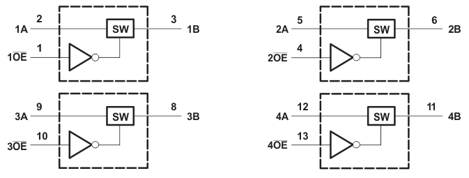
Logic Diagram (Positive Logic)

Pin numbers shown are for the DGV, PW, and RGY packages.
4 Revision History
Changes from B Revision (March 2005) to C Revision
- Added Pin Functions table, ESD Ratings table, Thermal Information table, Detailed Description section, Application and Implementation section, Power Supply Recommendations section, Layout section, Device and Documentation Support section, and Mechanical, Packaging, and Orderable Information sectionGo
- Deleted Ordering Information table.Go