SCDS008M May 1993 – June 2015 SN74CBT16214
PRODUCTION DATA.
- 1 Features
- 2 Applications
- 3 Description
- 4 Revision History
- 5 Pin Configuration and Functions
- 6 Specifications
- 7 Parameter Measurement Information
- 8 Detailed Description
- 9 Application and Implementation
- 10Power Supply Recommendations
- 11Layout
- 12Device and Documentation Support
- 13Mechanical, Packaging, and Orderable Information
パッケージ・オプション
デバイスごとのパッケージ図は、PDF版データシートをご参照ください。
メカニカル・データ(パッケージ|ピン)
- DGG|56
- DL|56
サーマルパッド・メカニカル・データ
発注情報
9 Application and Implementation
NOTE
Information in the following applications sections is not part of the TI component specification, and TI does not warrant its accuracy or completeness. TI’s customers are responsible for determining suitability of components for their purposes. Customers should validate and test their design implementation to confirm system functionality.
9.1 Application Information
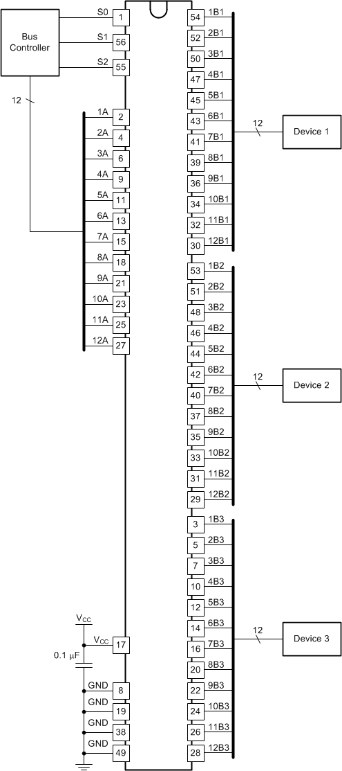
The SN74CBT16214 is typically used to expand a single 12-bit bus to three separate 12-bit busses. Fewer bits can be used as well if the unused inputs are tied to either ground or VCC.
9.2 Typical Application
 Figure 3. Typical Application Simplified Schematic
9.2.1 Design Requirements
The 0.1-uF capacitor should be placed as close as possible to the VCC pin of the device.
9.2.2 Detailed Design Procedure
- Recommended Input Conditions
- For switch time specifications, see propagation delay times in Switching Characteristics.
- Inputs should remain between 0.5 V and 7 V, regardless of VCC.
- For input voltage level specifications for control inputs, see VIH and VIL in Recommended Operating Conditions.
- Input/output current consideration: The SN74CBT16214 does not have internal current drive circuitry and thus cannot sink or source current. Any current will be passed through the device.
9.2.3 Application Curve
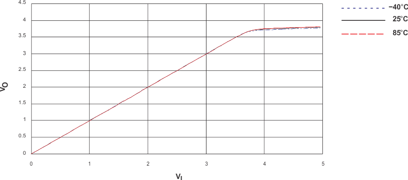
 Figure 4. VO vs VI, VCC = 5 V