SCDS019M May 1995 – December 2015 SN74CBT3251
PRODUCTION DATA.
- 1 Features
- 2 Applications
- 3 Description
- 4 Revision History
- 5 Pin Configuration and Functions
- 6 Specifications
- 7 Parameter Measurement Information
- 8 Detailed Description
- 9 Application and Implementation
- 10Power Supply Recommendations
- 11Layout
- 12Device and Documentation Support
- 13Mechanical, Packaging, and Orderable Information
パッケージ・オプション
デバイスごとのパッケージ図は、PDF版データシートをご参照ください。
メカニカル・データ(パッケージ|ピン)
- PW|16
- DB|16
- DBQ|16
- RGY|16
- D|16
サーマルパッド・メカニカル・データ
- RGY|16
発注情報
8 Detailed Description
8.1 Overview
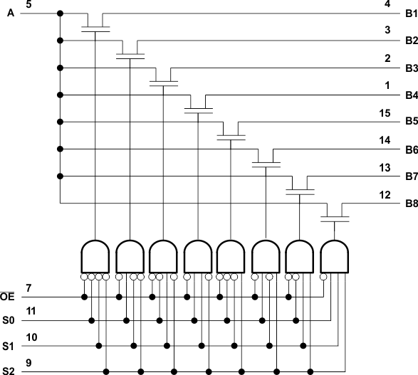
The SN74CBT3251 device is a single 8-channel multiplexer with three binary control inputs, S0, S1, and S2 and an OE (output enable, active low) input. The three binary signals select 1 of 8 channels to be turned on, and connect one of the 8 inputs to the output.
When they are used as demultiplexers, the CHANNEL IN/OUT terminals (B) are the outputs and the COMMON OUT/IN terminal (A) is the input.
8.2 Functional Block Diagram
 Figure 3. Logic Diagram (Positive Logic)
8.3 Feature Description
The SN74CBT3251 1-of-8 FET multiplexers and demultiplexers can accept a wide range of analog signal levels from 0 V to 5 V. It has low Ron resistance, typically 5-Ω for VCC = 5 V which allows very little signal loss through the switch. Binary address decoding on chip makes channel selection easy.
8.4 Device Functional Modes
Table 1 lists the functional modes of the SN74CBT3251.
Table 1. Function Table (Each Multiplexer and Demultiplexer)
| INPUTS | FUNCTION | |||
|---|---|---|---|---|
| OE | S2 | S1 | S0 | |
| L | L | L | L | A port = B1 port |
| L | L | L | H | A port = B2 port |
| L | L | H | L | A port = B3 port |
| L | L | H | H | A port = B4 port |
| L | H | L | L | A port = B5 port |
| L | H | L | H | A port = B6 port |
| L | H | H | L | A port = B7 port |
| L | H | H | H | A port = B8 port |
| H | X | X | X | Disconnect |