JAJSO60E March 1984 – February 2022 SN74HC682
PRODUCTION DATA
- 1 特長
- 2 概要
- 3 Revision History
- 4 Pin Configuration and Functions
- 5 Specifications
- 6 Parameter Measurement Information
- 7 Detailed Description
- 8 Power Supply Recommendations
- 9 Layout
- 10Device and Documentation Support
- 11Mechanical, Packaging, and Orderable Information
パッケージ・オプション
デバイスごとのパッケージ図は、PDF版データシートをご参照ください。
メカニカル・データ(パッケージ|ピン)
- N|20
- DW|20
サーマルパッド・メカニカル・データ
発注情報
2 概要
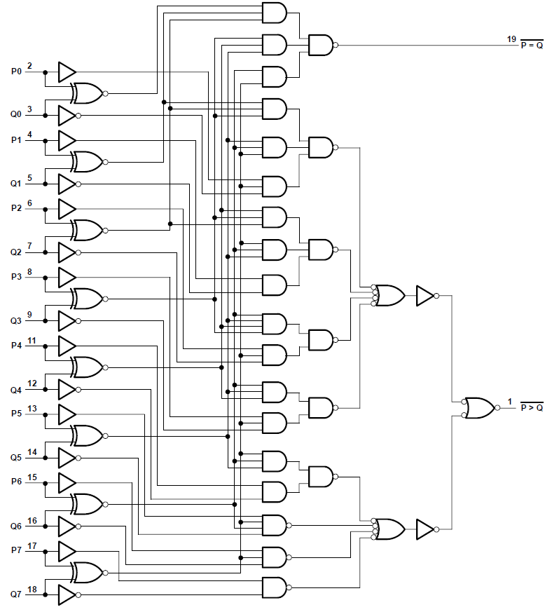
これらのマグニチュード・コンパレータは、2 つの 8 ビット・バイナリ・ワードまたは BCD ワードの比較を実行します。’HC682 デバイスは、アナログまたはスイッチ・データのために、Q 入力に 100kΩ のプルアップ終端抵抗を備えています。
製品情報
| 部品番号 | パッケージ(1) | 本体サイズ (公称) |
|---|---|---|
| SN74HC682DW | SOIC (20) | 12.8mm × 7.50mm |
| SN74HC682N | PDIP (20) | 25.40mm × 6.35mm |
(1) 利用可能なパッケージについては、このデータシートの末尾にある注文情報を参照してください。