JAJSHW1B
August 2019 – October 2019
SN74HCS7002-Q1
PRODUCTION DATA.
1
特長
2
アプリケーション
3
概要
Device Images
シュミットトリガ入力の利点
4
改訂履歴
5
Pin Configuration and Functions
Pin Functions
6
Specifications
6.1
Absolute Maximum Ratings
6.2
ESD Ratings
6.3
Recommended Operating Conditions
6.4
Thermal Information
6.5
Electrical Characteristics
6.6
Switching Characteristics
6.7
Typical Characteristics
7
Parameter Measurement Information
8
Detailed Description
8.1
Overview
8.2
Functional Block Diagram
8.3
Feature Description
8.3.1
Balanced CMOS Push-Pull Outputs
8.3.2
CMOS Schmitt-Trigger Inputs
8.3.3
Clamp Diode Structure
8.4
Device Functional Modes
9
Application and Implementation
9.1
Application Information
9.2
Typical Application
9.2.1
Design Requirements
9.2.1.1
Power Considerations
9.2.1.2
Input Considerations
9.2.1.3
Output Considerations
9.2.2
Detailed Design Procedure
9.2.3
Application Curves
10
Power Supply Recommendations
11
Layout
11.1
Layout Guidelines
11.2
Layout Example
12
デバイスおよびドキュメントのサポート
12.1
ドキュメントのサポート
12.1.1
関連資料
12.2
関連リンク
12.3
コミュニティ・リソース
12.4
商標
12.5
静電気放電に関する注意事項
12.6
Glossary
13
メカニカル、パッケージ、および注文情報
パッケージ・オプション
メカニカル・データ(パッケージ|ピン)
PW|14
MPDS360A
D|14
MPDS177H
サーマルパッド・メカニカル・データ
発注情報
jajshw1b_oa
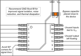
11.2
Layout Example
Figure 11.
Example layout for the SN74HCS7002
-Q1