JAJSNW5G November 1988 – October 2022 SN74HCT32
PRODUCTION DATA
- 1 特長
- 2 概要
- 3 Revision History
- 4 Pin Configuration and Functions
- 5 Specifications
- 6 Parameter Measurement Information
- 7 Detailed Description
- 8 Power Supply Recommendations
- 9 Layout
- 10Device and Documentation Support
- 11Mechanical, Packaging, and Orderable Information
パッケージ・オプション
デバイスごとのパッケージ図は、PDF版データシートをご参照ください。
メカニカル・データ(パッケージ|ピン)
- D|14
- PW|14
- DB|14
- N|14
- NS|14
サーマルパッド・メカニカル・データ
発注情報
6 Parameter Measurement Information
Phase relationships between waveforms were chosen arbitrarily. All input pulses are supplied by generators having the following characteristics: PRR ≤ 1 MHz, ZO = 50 Ω, tt < 6 ns.
For clock inputs, fmax is measured when the input duty cycle is 50%.
The outputs are measured one at a time with one input transition per measurement.

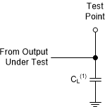
(1) CL includes probe
and test-fixture capacitance.
Figure 6-1 Load Circuit for Push-Pull
Outputs
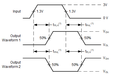
(1) The greater between
tPLH and tPHL is the same as
tpd.
Figure 6-2 Voltage Waveforms,
Propagation Delays for TTL-Compatible Inputs