SCLS467F FEBRUARY 2003 – June 2016 SN74LV123A-Q1
PRODUCTION DATA.
- 1 Features
- 2 Applications
- 3 Description
- 4 Revision History
- 5 Pin Configuration and Functions
-
6 Specifications
- 6.1 Absolute Maximum Ratings
- 6.2 ESD Ratings
- 6.3 Recommended Operating Conditions
- 6.4 Thermal Information
- 6.5 Electrical Characteristics
- 6.6 Timing Requirements — VCC = 3.3 V ± 0.3 V
- 6.7 Timing Requirements — VCC = 5 V ± 0.5 V
- 6.8 Switching Characteristics — VCC = 3.3 V ± 0.3 V
- 6.9 Switching Characteristics — VCC = 5 V ± 0.5 V
- 6.10 Operating Characteristics
- 6.11 Typical Characteristics
- 7 Parameter Measurement Information
- 8 Detailed Description
- 9 Application and Implementation
- 10Power Supply Recommendations
- 11Layout
- 12Device and Documentation Support
- 13Mechanical, Packaging, and Orderable Information
パッケージ・オプション
デバイスごとのパッケージ図は、PDF版データシートをご参照ください。
メカニカル・データ(パッケージ|ピン)
- PW|16
サーマルパッド・メカニカル・データ
発注情報
7 Parameter Measurement Information
 Figure 6. Load Circuit
 Figure 7. Voltage Waveforms Pulse Duration
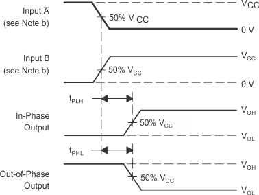
 Figure 8. Voltage Waveforms Delay Times
 Figure 9. Voltage Waveforms Delay Times
- CL includes probe and jig capacitance.
- All input pulses are supplied by generators having the following characteristics: PRR ≤ 1 MHz, ZO = 50 Ω, tr = 3 ns, tf = 3 ns.
- The outputs are measured one at a time, with one input transition per measurement.