JAJSR27D July 2003 – August 2023 SN74LV32A-Q1
PRODUCTION DATA
- 1
- 1特長
- 2概要
- 3Revision History
- 4Pin Configuration and Functions
-
5Specifications
- 5.1 Absolute Maximum Ratings
- 5.2 ESD Ratings
- 5.3 Recommended Operating Conditions
- 5.4 Thermal Information
- 5.5 Electrical Characteristics
- 5.6 Switching Characteristics, VCC = 2.5 V ±0.2 V
- 5.7 Switching Characteristics, VCC = 3.3 V ±0.3 V
- 5.8 Switching Characteristics, VCC = 5 V ±0.5 V
- 5.9 Noise Characteristics
- 5.10 Operating Characteristics
- 6Parameter Measurement Information
- 7Detailed Description
- 8Device and Documentation Support
- 9Mechanical, Packaging, and Orderable Information
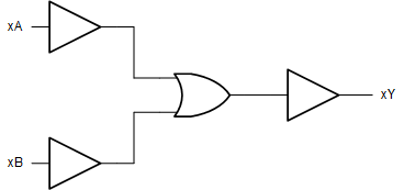
7.2 Functional Block Diagram
 Figure 7-1 Logic Diagram,
Each Gate (Positive Logic)