JAJSPY4D july 2003 – march 2023 SN74LV393A-Q1
PRODMIX
- 1 特長
- 2 アプリケーション
- 3 説明
- 4 Revision History
- 5 Pin Configuration and Functions
-
6 Specifications
- 6.1 Absolute Maximum Ratings
- 6.2 ESD Ratings
- 6.3 Recommended Operating Conditions
- 6.4 Thermal Information
- 6.5 Electrical Characteristics
- 6.6 Timing Requirements, VCC = 2.5 V ± 0.2 V
- 6.7 Timing Requirements, VCC = 3.3 V ± 0.3 V
- 6.8 Timing Requirements, VCC = 5 V ± 0.5 V
- 6.9 Switching Characteristics, VCC = 2.5 V ± 0.2 V
- 6.10 Switching Characteristics, VCC = 3.3 V ± 0.3 V
- 6.11 Switching Characteristics, VCC = 5 V ± 0.5 V
- 6.12 Noise Characteristics
- 6.13 Operating Characteristics
- 7 Parameter Measurement Information
- 8 Detailed Description
- 9 Application and Implementation
- 10Device and Documentation Support
- 11Mechanical, Packaging, and Orderable Information
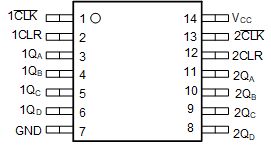
5 Pin Configuration and Functions
 Figure 5-1 PW Package, 14-Pin TSSOP (Top
View)
Figure 5-1 PW Package, 14-Pin TSSOP (Top
View)Table 5-1 Pin Functions
| PIN | TYPE(1) | DESCRIPTION | |
|---|---|---|---|
| NAME | NO. | ||
| 1CLK/ | 1 | I | Counter 1 Clock Input |
| 1CLR | 2 | I | Counter 1 Clear Input |
| 1QA | 3 | O | Counter 1 A Output |
| 1QB | 4 | O | Counter 1 B Output |
| 1QC | 5 | O | Counter 1 B Output |
| 1QD | 6 | O | Counter 1 B Output |
| GND | 7 | G | Ground |
| 2QD | 8 | O | Counter 2 D Output |
| 2QC | 9 | O | Counter 2 C Output |
| 2QB | 10 | O | Counter 2 B Output |
| 2QA | 11 | O | Counter 2 A Output |
| 2CLR | 12 | I | Counter 2 Clear Input |
| 2CLK/ | 13 | I | Counter 2 Clock Input |
| VCC | 14 | P | VCC |
(1) I = Input, O = Output, I/O =
Input or Output, G = Ground, P = Power.