SCES656E February 2006 – November 2016 SN74LV4046A
PRODUCTION DATA.
- 1 Features
- 2 Applications
- 3 Description
- 4 Revision History
- 5 Pin Configuration and Functions
- 6 Specifications
- 7 Detailed Description
- 8 Application and Implementation
- 9 Power Supply Recommendations
- 10Layout
- 11Device and Documentation Support
- 12Mechanical, Packaging, and Orderable Information
パッケージ・オプション
メカニカル・データ(パッケージ|ピン)
サーマルパッド・メカニカル・データ
発注情報
6 Specifications
6.1 Absolute Maximum Ratings
over operating free-air temperature range (unless otherwise noted)(1)| MIN | MAX | UNIT | |||
|---|---|---|---|---|---|
| VCC | DC supply voltage | –0.5 | 7 | V | |
| VI | Input voltage | –0.5 | VCC + 0.5 | V | |
| VO | Output voltage | –0.5 | VCC + 0.5 | V | |
| IIK | Input clamp current | VI < 0 | –20 | mA | |
| IOK | Output clamp current | VO < 0 | –50 | mA | |
| IO | Continuous output curent | VO = 0 to VCC | ±35 | mA | |
| ICC | DC VCC or ground current | ±70 | mA | ||
| TJ | Junction temperature | 150 | °C | ||
| Tstg | Storage temperature | –65 | 150 | °C | |
(1) Stresses beyond those listed under Absolute Maximum Ratings may cause permanent damage to the device. These are stress ratings only, and functional operation of the device at these or any other conditions beyond those indicated under Recommended Operating Conditions is not implied. Exposure to absolute-maximum-rated conditions for extended periods may affect device reliability.
6.2 ESD Ratings
| VALUE | UNIT | |||
|---|---|---|---|---|
| V(ESD) | Electrostatic discharge | Human body model (HBM), per ANSI/ESDA/JEDEC JS-001(1) | ±2000 | V |
| Charged-device model (CDM), per JEDEC specification JESD22-C101(2) | ±1000 | |||
(1) JEDEC document JEP155 states that 500-V HBM allows safe manufacturing with a standard ESD control process.
(2) JEDEC document JEP157 states that 250-V CDM allows safe manufacturing with a standard ESD control process.
6.3 Recommended Operating Conditions
over operating free-air temperature range (unless otherwise noted)| MIN | MAX | UNIT | ||
|---|---|---|---|---|
| TA | Operating free-air temperature | –40 | 125 | °C |
| VCC | Supply voltage | 3 | 5.5 | V |
| VI, VO | DC input or output voltage | 0 | VCC | V |
6.4 Thermal Information
| THERMAL METRIC(1) | SN74LV4046A | UNIT | |||||
|---|---|---|---|---|---|---|---|
| D (SOIC) | DGV (TVSOP) | NS (SO) | PW (TSSOP) | N (PDIP) | |||
| 16 PINS | 16 PINS | 16 PINS | 16 PINS | 16 PINS | |||
| RθJA | Junction-to-ambient thermal resistance | 82.8 | 116.8 | 83.5 | 108.1 | 49.4 | °C/W |
| RθJC(top) | Junction-to-case (top) thermal resistance | 44.0 | 43.3 | 41.7 | 42.7 | 36.7 | °C/W |
| RθJB | Junction-to-board thermal resistance | 40.3 | 48.3 | 43.8 | 53.1 | 29.3 | °C/W |
| ψJT | Junction-to-top characterization parameter | 11.1 | 3.7 | 9.3 | 4.2 | 21.5 | °C/W |
| ψJB | Junction-to-board characterization parameter | 40.0 | 47.8 | 43.5 | 52.5 | 29.2 | °C/W |
(1) For more information about traditional and new thermal metrics, see the Semiconductor and IC Package Thermal Metrics application report.
6.5 Electrical Characteristics
over operating free-air temperature range (unless otherwise noted)| PARAMETER | TEST CONDITIONS | VCC (V) | MIN | TYP | MAX | UNIT | ||||
|---|---|---|---|---|---|---|---|---|---|---|
| VI (V) | IO (mA) | |||||||||
| VCO | ||||||||||
| VIH | High-level input voltage | INH | 3 to 3.6 | VCC × 0.7 | V | |||||
| 4.5 to 5.5 | VCC × 0.7 | |||||||||
| VIL | Low-level input voltage | INH | 3 to 5.5 | VCC × 0.3 | V | |||||
| 4.5 to 5.5 | VCC × 0.3 | |||||||||
| VOH | High-level output voltage |
VCOOUT | CMOS | VIL or VIH | –0.05 | 3 to 3.6 | VCC – 0.1 | V | ||
| 4.5 to 5.5 | VCC – 0.1 | |||||||||
| TTL | –12 | 4.5 to 5.5 | 3.8 | |||||||
| VOL | Low-level output voltage |
VCOOUT | CMOS | VIL or VIH | 0.05 | 3 to 3.6 | 0.1 | V | ||
| 4.5 to 5.5 | 0.1 | |||||||||
| TTL | 12 | 4.5 to 5.5 | 0.55 | |||||||
| C1A, C1B (test purposes only) |
12 | 4.5 to 5.5 | 0.65 | |||||||
| II | Input leakage current | INH, VCOIN | VCC or GND | 5.5 | ±1 | μA | ||||
| R1 range(1) | 3 to 5.5 | 3 | 50 | kΩ | ||||||
| R2 range(1) | 3 to 5.5 | 3 | 50 | kΩ | ||||||
| C1 capacitance range | 3 to 3.6 | 40 | No Limit | pF | ||||||
| 4.5 to 5.5 | 40 | No Limit | ||||||||
| Operating voltage range | VCOIN | Over the range specified for R1 for linearity(2) | 3 to 3.6 | 1.1 | 1.9 | V | ||||
| 4.5 to 5.5 | 1.1 | 3.2 | ||||||||
| PHASE COMPARATOR | ||||||||||
| VIH | DC-coupled high-level input voltage |
SIGIN, COMPIN | 3 to 3.6 | VCC × 0.7 | ||||||
| 4.5 to 5.5 | VCC × 0.7 | |||||||||
| VIL | DC-coupled low-level input voltage | SIGIN, COMPIN | 3 to 3.6 | VCC × 0.3 | V | |||||
| 4.5 to 5.5 | VCC × 0.3 | |||||||||
| VOH | High-level output voltage |
PCPOUT, PCNOUT | CMOS | VIL or VIH | –0.05 | 3 to 5.5 | VCC – 0.1 | V | ||
| –6 | 3 to 3.6 | 2.48 | ||||||||
| TTL | –12 | 4.5 to 5.5 | 3.8 | |||||||
| VOL | Low-level output voltage |
PCPOUT, PCNOUT | CMOS | VIL or VIH | 0.02 | 3 to 3.6 | 0.1 | V | ||
| 4.5 to 5.5 | 0.1 | |||||||||
| 4 | 4.5 to 5.5 | 0.4 | ||||||||
| TTL | ||||||||||
| II | Input leakage current | SIGIN, COMPIN | VCC or GND | 3 to 3.6 | ±11 | μA | ||||
| 4.5 to 5.5 | ±29 | |||||||||
| IOZ | 3-state off-state current | PC2OUT | VIL or VIH | 3 to 5.5 | ±5 | μA | ||||
| RI | Input resistance | SIGIN, COMPIN | VI at self-bias operating point, VI = 0.5 V | 3 | 800 | kΩ | ||||
| 4.5 | 250 | |||||||||
| DEMODULATOR | ||||||||||
| RS | Resistor range | RS > 300 kΩ, Leakage current can influence VDEMOUT | 3 to 3.6 | 50 | 300 | kΩ | ||||
| 4.5 to 5.5 | 50 | 300 | ||||||||
| VOFF | Offset voltage VCOIN to VDEM | VI = VVCOIN = VCC/2, Values taken over RS range | 3 to 3.6 | ±30 | mV | |||||
| 4.5 to 5.5 | ±20 | |||||||||
| ICC | Quiescent device current | Pins 3, 5, and 14 at VCC, Pin 9 at GND, II at pins 3 and 14 to be excluded |
5.5 | 50 | μA | |||||
(1) The value for R1 and R2 in parallel should exceed 2.7 kΩ.
(2) The maximum operating voltage can be as high as VCC – 0.9 V; however, this may result in an increased offset voltage.
6.6 Switching Characteristics
over operating free-air temperature range (unless otherwise noted) CL = 50 pF, Input tr, tf = 6 ns| PARAMETER | TEST CONDITIONS | VCC
(V) |
MIN | TYP | MAX | UNIT | ||
|---|---|---|---|---|---|---|---|---|
| PHASE COMPARATOR | ||||||||
| tPLH, tPHL | Propagation delay | SIGIN, COMPIN to PC1OUT | 3 to 3.6 | 135 | ns | |||
| 4.5 to 5.5 | 50 | |||||||
| tPLH, tPHL | Propagation delay | SIGIN, COMPIN to PCPOUT | 3 to 3.6 | 300 | ns | |||
| 4.5 to 5.5 | 60 | |||||||
| tPLH, tPHL | Propagation delay | SIGIN, COMPIN to PC3OUT | 3 to 3.6 | 200 | ns | |||
| 4.5 to 5.5 | 50 | |||||||
| tTHL, tTLH | Output transition time | 3 to 3.6 | 75 | ns | ||||
| 4.5 to 5.5 | 15 | |||||||
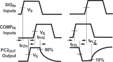
| tPZH, tPZL | 3-state output enable time | SIGIN, COMPIN to PC2OUT | 3 to 3.6 | 270 | ns | |||
| 4.5 to 5.5 | 54 | |||||||
| tPHZ, tPLZ | 3-state output disable time | SIGIN, COMPIN to PC2OUT | 3 to 3.6 | 320 | ns | |||
| 4.5 to 5.5 | 65 | |||||||
| AC-coupled input sensitivity | (P-P) at SIGIN or COMPIN | VI(P-P) | 3 to 3.6 | 11 | mV | |||
| 4.5 to 5.5 | 15 | |||||||
| VCO | ||||||||
| Δf/ΔT | Frequency stability with temperature change | VI = VCOIN = 1/2 VCC, R1 = 100 kΩ, R2 = ∞, C1 = 100 pF |
3 to 3.6 | 0.11 | %/°C | |||
| 4.5 to 5.5 | 0.11 | |||||||
| fMAX | Maximum frequency | C1 = 50 pF, R1 = 3.5 kΩ, R2 = ∞ |
3 to 3.6 | 24 | MHz | |||
| 4.5 to 5.5 | 24 | |||||||
| C1 = 0 pF, R1 = 9.1 kΩ, R2 = ∞ |
3 to 3.6 | 38 | ||||||
| 4.5 to 5.5 | 38 | |||||||
| Center frequency (duty 50%) | C1 = 40 pF, R1 = 3 kΩ, R2 = ∞, VCOIN = VCC/2 |
3 to 3.6 | 7 | 10 | MHz | |||
| 4.5 to 5.5 | 12 | 17 | ||||||
| 4.5(1) | 15(1) | 17.5(1) | ||||||
| ΔfVCO | Frequency linearity | C1 = 100 pF, R1 = 100 kΩ, R2 = ∞ |
3 to 3.6 | 0.4% | ||||
| 4.5 to 5.5 | 0.4% | |||||||
| Offset frequency | C1 = 1 nF, R2 = 220 kΩ |
3 to 3.6 | 400 | kHz | ||||
| 4.5 to 5.5 | 400 | |||||||
| DEMODULATOR | ||||||||
| VOUT vs fIN | C1 = 100 pF, C2 = 100 pF, R1 = 100 kΩ, R2 = ∞, R3 = 100 kΩ |
3 | 8 | mV/kHz | ||||
| 4.5 | 330 | |||||||
(1) Data is specified at 25°C
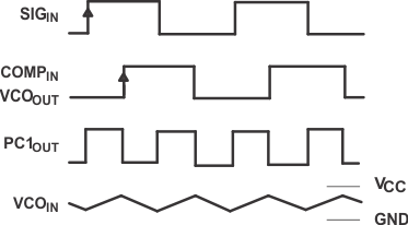
| Loop Locked at fo |
Phase Comparator 1
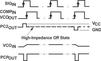
| Loop Locked at fo |
Phase Comparator 2
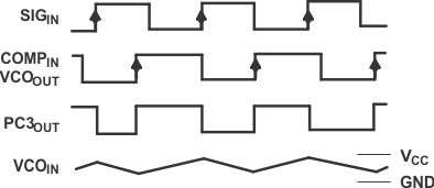
| Loop Locked at fo |
Phase Comparator 3
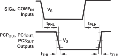
Output Transition Times
6.7 Typical Characteristics
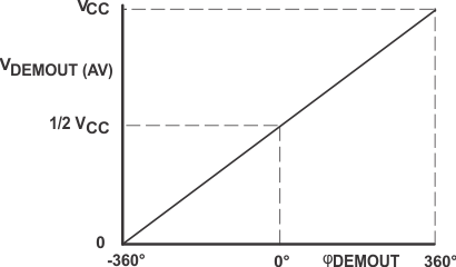
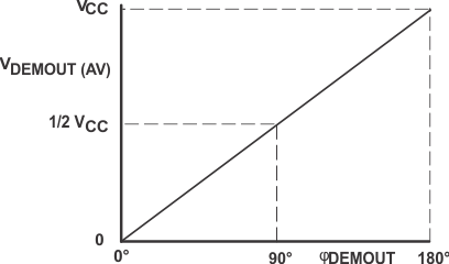 Figure 6. Average Output Voltage vs Input Phase Difference
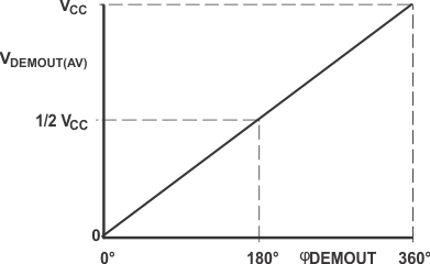
| Phase Comparator 3: | ||
| VDEMOUT = VPC3OUT = (VCC/2π) (SIGIN – COMPIN); | ||
| DEMOUT = (SIGIN – COMPIN) |
